Hybrid-pi model: Difference between revisions
imported>John R. Brews No edit summary |
mNo edit summary |
||
| (25 intermediate revisions by one other user not shown) | |||
| Line 2: | Line 2: | ||
{{TOC|right}} | {{TOC|right}} | ||
The '''hybrid-pi model''' is a popular [[circuit]] model used for analyzing the | The '''hybrid-pi model''' is a popular [[Electrical circuit|circuit]] model used for analyzing the small-signal behavior of [[transistors]]. The hybrid-pi models apply only to devices in [[Mode (electronics)|''active'' mode]]; that is, the DC biases are applied to set the operating point or Q-point in the normal operating regime for analog circuit operation.<ref name=mode/> The model can be quite accurate for low-frequency operation and can be adapted for higher frequency operation by addition of inter-electrode [[capacitance]]s and other parasitic elements. | ||
==Bipolar transistor== | ==Bipolar transistor== | ||
{{main|Bipolar transistor}} | |||
{{Image|Bipolar hybrid-pi model.PNG|right|200px| Simplified, low-frequency hybrid-pi [[BJT]] model.}} | {{Image|Bipolar hybrid-pi model.PNG|right|200px| Simplified, low-frequency hybrid-pi [[BJT]] model.}} | ||
{{Image|Bipolar hybrid-pi | {{Image|Bipolar hybrid-pi as two-port.PNG|right|350px|The bipolar hybrid-pi model interpreted as a ''y''-parameter two-port. The emitter node is split artificially to satisfy the port conditions.}} | ||
The hybrid-pi model is a linearized | |||
The hybrid-pi model is a linearized three-terminal approximation to the transistor using the small-signal base-emitter voltage ''v<sub>π</sub>'' and collector-emitter voltage ''v<sub>ce</sub>'' as independent variables, and the small-signal base current ''i<sub>b</sub>'' and collector current ''i<sub>c</sub>'' as dependent variables. | |||
A basic, low-frequency hybrid-pi model for the [[bipolar transistor]] is shown in the figure. The three transistor terminals are ''E'' = emitter, ''B'' = base, and ''C'' = collector. The base-emitter connection is through a resistor ''r<sub>π</sub>'', and the base current causes a small-signal voltage drop across it, ''v<sub>π</sub>'' (the π notation is standard). Voltage ''v<sub>π</sub>'' induces a small-signal collector current ''via'' the voltage-controlled current source with current ''g<sub>m</sub>v<sub>π</sub>'', ''g<sub>m</sub>'' is the transistor ''transconductance''. | A basic, low-frequency hybrid-pi model for the [[bipolar transistor]] is shown in the figure. The three transistor terminals are ''E'' = emitter, ''B'' = base, and ''C'' = collector. The base-emitter connection is through a resistor ''r<sub>π</sub>'', and the base current causes a small-signal voltage drop across it, ''v<sub>π</sub>'' (the π notation is standard). Voltage ''v<sub>π</sub>'' induces a small-signal collector current ''via'' the voltage-controlled current source with current ''g<sub>m</sub>v<sub>π</sub>'', ''g<sub>m</sub>'' is the transistor ''transconductance''. | ||
This three-terminal model can be viewed as a [[Two-port_network#Admittance_parameters_.28y-parameters.29|''y''-parameter two-port network]], as shown in the next figure. However, to qualify as a port, current into and out of the two terminals of a port must be the same. To meet this requirement, a mathematical artifice is introduced of splitting of the emitter current into separate base and collector currents, which does not correspond to any physical phenomenon.<ref name=Jaeger1/> If this two-port is inserted into a larger circuit, the input and output port conditions will be violated if the connected circuitry does not itself satisfy the port conditions. To elaborate: this four-terminal model of the bipolar transistor does not ''enforce'' the port conditions, it is only ''compatible'' with them if they are requested by the surrounding circuitry. | |||
Equivalence to the three-terminal circuit is established using the relations ''v<sub>π</sub> = i<sub>b</sub>r<sub>π</sub>'' and ''β = g<sub>m</sub>r<sub>π</sub>''. Thus, the dependent source current ''g<sub>m</sub>v<sub>π</sub> = βi<sub>b</sub>'', and is the same in both circuits. | |||
The various parameters are as follows. | The various parameters are as follows. | ||
| Line 23: | Line 29: | ||
*<math> r_O = \frac{v_{ce}}{i_{c}}\Bigg |_{v_{be}=0} = \begin{matrix}\frac {V_A+V_{CE}}{I_C}\end{matrix} \approx \begin{matrix} \frac {V_A}{I_C}\end{matrix}</math> is the output resistance due to the [[Early effect]], and ''V<sub>A</sub>'' is called the ''Early voltage''. | *<math> r_O = \frac{v_{ce}}{i_{c}}\Bigg |_{v_{be}=0} = \begin{matrix}\frac {V_A+V_{CE}}{I_C}\end{matrix} \approx \begin{matrix} \frac {V_A}{I_C}\end{matrix}</math> is the output resistance due to the [[Early effect]], and ''V<sub>A</sub>'' is called the ''Early voltage''. | ||
=== | ===''Related parameters''=== | ||
The reciprocal of the output resistance is named the '''output conductance''' | The reciprocal of the output resistance is named the '''output conductance''' | ||
:*<math>g_{ce} = \frac {1} {r_O} </math>. | :*<math>g_{ce} = \frac {1} {r_O} </math>. | ||
| Line 32: | Line 35: | ||
The reciprocal of g<sub>m</sub> is called the '''intrinsic resistance''' | The reciprocal of g<sub>m</sub> is called the '''intrinsic resistance''' | ||
:*<math>r_{E} = \frac {1} {g_m} </math>. | :*<math>r_{E} = \frac {1} {g_m} </math>. | ||
===Higher frequencies=== | |||
{{Image|Bipolar hybrid-pi capacitances.PNG|right|300px|Bipolar hybrid-pi model with parasitic capacitances to model frequency dependence.}} | |||
As frequencies are increased, amplifier gain drops off with increasing frequency because the bipolar transistor is degraded by parasitic capacitances. These effects must be modeled to assess the limitations of bipolar circuits. Three parasitic elements are commonly added to the hybrid-pi model to make frequency predictions. One is the base-emitter capacitance ''C<sub>π</sub>'', which includes the base-emitter [[diffusion capacitance]] and the base-emitter junction capacitance. At high enough frequencies, ''C<sub>π</sub>'' shorts out the transistor and it fails to function. A second parasitic capacitance ''C<sub>μ</sub>'' connects the base to the collector. Because the base-collector junction is reverse biased in active mode, there is no diffusion capacitance in this case, and this capacitance represents the emitter-base junction capacitance alone. Although this capacitor is small, its influence is multiplied by the transistor gain which amplifies the voltage variation at the base connection and applies it to the collector connection, exaggerating the influence of this capacitor through the [[Miller effect]]. The small series base resistance ''r<sub>x</sub>'' plays a role only when there is no other resistance introduced by the circuit into the base lead. For example, if the base is grounded, the presence of ''r<sub>X</sub>'' means the top of the base resistance ''r<sub>π</sub>'' is ''not'' at AC ground, and can develop a transient voltage, which in turn can enable gain roll-off due to the [[Miller effect]] capacitance. | |||
==MOSFET == | ==MOSFET == | ||
{{main|MOSFET}} | |||
{{Image|MOSFET hybrid-pi with capactances.PNG|right|300px|Simplified, three-terminal MOSFET hybrid-pi model.}} | {{Image|MOSFET hybrid-pi with capactances.PNG|right|300px|Simplified, three-terminal MOSFET hybrid-pi model.}} | ||
{{Image|MOSFET four-terminal hybrid-pi circuit.PNG|right|350px|Four-terminal small-signal MOSFET circuit.}} | {{Image|MOSFET four-terminal hybrid-pi circuit.PNG|right|350px|Four-terminal small-signal MOSFET circuit.}} | ||
| Line 42: | Line 50: | ||
*<math>g_m = \frac{i_{d}}{v_{gs}}\Bigg |_{v_{ds}=0}</math> | *<math>g_m = \frac{i_{d}}{v_{gs}}\Bigg |_{v_{ds}=0}</math> | ||
is the [[transconductance]] in [[Siemens (unit)|siemens]], | is the [[transconductance]] in [[Siemens (unit)|siemens]]. The various parameters can be evaluated using a variety of models.<ref name=model/> For example, with the Shichman-Hodges model, in terms of the quiescent point (that is, zero signal) drain current <math> I_D</math>, one finds:<ref name=Jaeger2/>: | ||
:::<math>\ g_m = \begin{matrix}\frac {2I_\mathrm{D}}{ V_{\mathrm{GS}}-V_\mathrm{th} }\end{matrix}</math>, | :::<math>\ g_m = \begin{matrix}\frac {2I_\mathrm{D}}{ V_{\mathrm{GS}}-V_\mathrm{th} }\end{matrix}</math>, | ||
| Line 68: | Line 76: | ||
It must be pointed out that the Shichman-Hodges model for voltage and geometry dependence of the device parameters such as ''g<sub>m</sub>'', ''r<sub>O</sub>'' has absolutely no claim to accuracy, especially in today's technology. However, it still is widely used in textbooks to get the flavor of MOSFET circuit design. Nobody would actually implement a circuit expecting this model to be quantitative, however, and real design work always involves extensive computer modeling, for example, using the BSIM computer model.<ref name=BSIM/> | It must be pointed out that the Shichman-Hodges model for voltage and geometry dependence of the device parameters such as ''g<sub>m</sub>'', ''r<sub>O</sub>'' has absolutely no claim to accuracy, especially in today's technology. However, it still is widely used in textbooks to get the flavor of MOSFET circuit design. Nobody would actually implement a circuit expecting this model to be quantitative, however, and real design work always involves extensive computer modeling, for example, using the BSIM computer model.<ref name=BSIM/> | ||
The lower figure explicitly introduces the body contact and the capacitances to the body. This circuit is a great deal more complicated than the three-terminal circuit, and is avoided where possible. However, in some circuits the body is not short-circuited to the source, and the body must be explicitly handled. Even at low frequencies the effect of the dependent source ''g<sub>mb</sub>v<sub>bs</sub>'' (the so-called "back gate") must be taken into account. | The small-signal circuit of the lower figure explicitly introduces the body contact and the capacitances to the body. This circuit is a great deal more complicated than the three-terminal circuit, and is avoided where possible. However, in some circuits the body is not short-circuited to the source, and the body must be explicitly handled. Even at low frequencies the effect of the dependent source ''g<sub>mb</sub>v<sub>bs</sub>'' (the so-called "back gate") must be taken into account. | ||
==References and notes== | ==References and notes== | ||
| Line 109: | Line 117: | ||
|page=§0124, p. 13 | |page=§0124, p. 13 | ||
|publisher=Springer | |publisher=Springer | ||
|location= | |location=Dordrecht | ||
|isbn=0-387-25746-2 | |isbn=0-387-25746-2 | ||
|url=http://worldcat.org/isbn/0387257462}} | |url=http://worldcat.org/isbn/0387257462}} | ||
| Line 119: | Line 127: | ||
</ref> | </ref> | ||
}} | <ref name=mode> | ||
For the bipolar transistor, active mode corresponds to quiescent (zero signal) operating conditions with a forward biased emitter-base junction and a reverse- or zero-biased collector base junction. For the MOSFET, active mode corresponds to a gate-to-source voltage above threshold ([[MOSFET#Operation|inversion layer]] present at the source-end of the channel), gate-to-drain voltage at or below threshold (no inversion layer at the drain end of the channel), zero-biased or reverse-biased source-to-body junction, and a drain-to-body reverse bias greater than or equal to the source-to-body reverse bias. The threshold voltage, which sets the onset of inversion-layer formation, is larger, the larger the source-to-body reverse bias. For example, see {{cite book |title=Microelectronic circuits |author=Adel S Sedra and Kenneth C Smith |edition=4rth ed |year=1998 |chapter= |publisher=Oxford University Press |isbn=0-19-511690-9}}: §4.4 "Circuit symbols and conventions", pp. 234 ''ff'' , for the bipolar transistor, and §5.2 "Current-voltage characteristics for the enhancement MOSFET", pp. 366 ''ff'', for the MOSFET. | |||
</ref> | |||
<ref name=model> | |||
A variety of models are in use for the MOSFET, and are routinely employed for circuit analysis by computer, commonly using the program generically known as SPICE. The Shichman-Hodges model is referred to in these programs as "Level 1". See, for example, {{cite book |title= Semiconductor Device Modeling with Spice |author=Giuseppe Massobrio, Paolo Antognetti |url=http://books.google.com/books?id=0TNetkitYb4C&pg=PA213 |pages=pp. 213 ''ff'' |chapter=§4.9: Small-signal models |isbn=0071349553 |year=1999 |publisher=McGraw-Hill Professional |edition=2nd ed}} These computer simulations also can handle large-signal operation. | |||
</ref> | |||
}}[[Category:Suggestion Bot Tag]] | |||
Latest revision as of 06:01, 30 August 2024
The hybrid-pi model is a popular circuit model used for analyzing the small-signal behavior of transistors. The hybrid-pi models apply only to devices in active mode; that is, the DC biases are applied to set the operating point or Q-point in the normal operating regime for analog circuit operation.[1] The model can be quite accurate for low-frequency operation and can be adapted for higher frequency operation by addition of inter-electrode capacitances and other parasitic elements.
Bipolar transistor
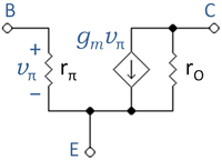
The hybrid-pi model is a linearized three-terminal approximation to the transistor using the small-signal base-emitter voltage vπ and collector-emitter voltage vce as independent variables, and the small-signal base current ib and collector current ic as dependent variables.
A basic, low-frequency hybrid-pi model for the bipolar transistor is shown in the figure. The three transistor terminals are E = emitter, B = base, and C = collector. The base-emitter connection is through a resistor rπ, and the base current causes a small-signal voltage drop across it, vπ (the π notation is standard). Voltage vπ induces a small-signal collector current via the voltage-controlled current source with current gmvπ, gm is the transistor transconductance.
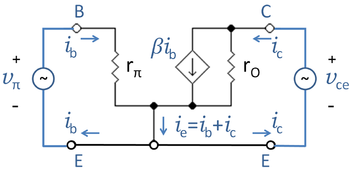
This three-terminal model can be viewed as a y-parameter two-port network, as shown in the next figure. However, to qualify as a port, current into and out of the two terminals of a port must be the same. To meet this requirement, a mathematical artifice is introduced of splitting of the emitter current into separate base and collector currents, which does not correspond to any physical phenomenon.[2] If this two-port is inserted into a larger circuit, the input and output port conditions will be violated if the connected circuitry does not itself satisfy the port conditions. To elaborate: this four-terminal model of the bipolar transistor does not enforce the port conditions, it is only compatible with them if they are requested by the surrounding circuitry.
Equivalence to the three-terminal circuit is established using the relations vπ = ibrπ and β = gmrπ. Thus, the dependent source current gmvπ = βib, and is the same in both circuits.
The various parameters are as follows.
- is the transconductance in siemens, evaluated in a simple model (see Jaeger and Blalock[3])
- where:
- is the quiescent collector current (also called the collector bias or DC collector current)
- is the thermal voltage, calculated from Boltzmann's constant, the charge on an electron, and the transistor temperature in kelvins. At 290 K (an approximation to room temperature: 70°F ≈ 294 K) VT is very nearly 25 mV (Google calculator).
- in ohms
- where:
- is the current gain at low frequencies (commonly called hFE). Here is the Q-point base current. This is a parameter specific to each transistor, and can be found on a datasheet; is a function of the choice of collector current.
- is the output resistance due to the Early effect, and VA is called the Early voltage.
Related parameters
The reciprocal of the output resistance is named the output conductance
- .
The reciprocal of gm is called the intrinsic resistance
- .
Higher frequencies
As frequencies are increased, amplifier gain drops off with increasing frequency because the bipolar transistor is degraded by parasitic capacitances. These effects must be modeled to assess the limitations of bipolar circuits. Three parasitic elements are commonly added to the hybrid-pi model to make frequency predictions. One is the base-emitter capacitance Cπ, which includes the base-emitter diffusion capacitance and the base-emitter junction capacitance. At high enough frequencies, Cπ shorts out the transistor and it fails to function. A second parasitic capacitance Cμ connects the base to the collector. Because the base-collector junction is reverse biased in active mode, there is no diffusion capacitance in this case, and this capacitance represents the emitter-base junction capacitance alone. Although this capacitor is small, its influence is multiplied by the transistor gain which amplifies the voltage variation at the base connection and applies it to the collector connection, exaggerating the influence of this capacitor through the Miller effect. The small series base resistance rx plays a role only when there is no other resistance introduced by the circuit into the base lead. For example, if the base is grounded, the presence of rX means the top of the base resistance rπ is not at AC ground, and can develop a transient voltage, which in turn can enable gain roll-off due to the Miller effect capacitance.
MOSFET
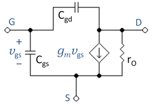
Unlike the bipolar transistor, the MOSFET fundamentally is a four-terminal, not a three-terminal, device, the terminals being S = source, D = drain, G = gate, and B = body or substrate. The body is not normally used deliberately as a signal node, and the analogy to the bipolar device is stretched a bit to minimize differences between these devices.
The upper figure shows the three-terminal small-signal equivalent circuit for the MOSFET, which ignores the body contact altogether, anticipating it is short-circuited to the source. At low frequencies,the capacitances all are replaced with open circuits to obtain a frequency-independent circuit depending upon resistors only. The various parameters are as follows.
is the transconductance in siemens. The various parameters can be evaluated using a variety of models.[4] For example, with the Shichman-Hodges model, in terms of the quiescent point (that is, zero signal) drain current , one finds:[5]:
- ,
- where:
- is the quiescent drain current (also called the drain bias or DC drain current)
- = threshold voltage and = gate-to-source voltage.
The combination:
often is called the overdrive voltage.
- is the output resistance due to channel length modulation, calculated using the Shichman-Hodges model as
- ,
using the approximation for the channel length modulation parameter λ[6]
- .
Here VE is a technology related parameter (about 4 V / μm for the 65 nm technology node[6]) and L is the length of the source-to-drain separation.
The reciprocal of the output resistance is named the drain conductance
- .
It must be pointed out that the Shichman-Hodges model for voltage and geometry dependence of the device parameters such as gm, rO has absolutely no claim to accuracy, especially in today's technology. However, it still is widely used in textbooks to get the flavor of MOSFET circuit design. Nobody would actually implement a circuit expecting this model to be quantitative, however, and real design work always involves extensive computer modeling, for example, using the BSIM computer model.[7]
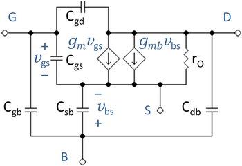
The small-signal circuit of the lower figure explicitly introduces the body contact and the capacitances to the body. This circuit is a great deal more complicated than the three-terminal circuit, and is avoided where possible. However, in some circuits the body is not short-circuited to the source, and the body must be explicitly handled. Even at low frequencies the effect of the dependent source gmbvbs (the so-called "back gate") must be taken into account.
References and notes
- ↑ For the bipolar transistor, active mode corresponds to quiescent (zero signal) operating conditions with a forward biased emitter-base junction and a reverse- or zero-biased collector base junction. For the MOSFET, active mode corresponds to a gate-to-source voltage above threshold (inversion layer present at the source-end of the channel), gate-to-drain voltage at or below threshold (no inversion layer at the drain end of the channel), zero-biased or reverse-biased source-to-body junction, and a drain-to-body reverse bias greater than or equal to the source-to-body reverse bias. The threshold voltage, which sets the onset of inversion-layer formation, is larger, the larger the source-to-body reverse bias. For example, see Adel S Sedra and Kenneth C Smith (1998). Microelectronic circuits, 4rth ed. Oxford University Press. ISBN 0-19-511690-9. : §4.4 "Circuit symbols and conventions", pp. 234 ff , for the bipolar transistor, and §5.2 "Current-voltage characteristics for the enhancement MOSFET", pp. 366 ff, for the MOSFET.
- ↑ R.C. Jaeger and T.N. Blalock (2004). Microelectronic Circuit Design, Second Edition. New York: McGraw-Hill, Section 13.5, esp. Eqs. 13.19. ISBN 0-07-232099-0.
- ↑ R.C. Jaeger and T.N. Blalock. Eq. 5.45 pp. 242 and Eq. 13.25 p. 682. ISBN 0-07-232099-0.
- ↑ A variety of models are in use for the MOSFET, and are routinely employed for circuit analysis by computer, commonly using the program generically known as SPICE. The Shichman-Hodges model is referred to in these programs as "Level 1". See, for example, Giuseppe Massobrio, Paolo Antognetti (1999). “§4.9: Small-signal models”, Semiconductor Device Modeling with Spice, 2nd ed. McGraw-Hill Professional, pp. 213 ff. ISBN 0071349553. These computer simulations also can handle large-signal operation.
- ↑ R.C. Jaeger and T.N. Blalock. Eq. 4.20 pp. 155 and Eq. 13.74 p. 702. ISBN 0-07-232099-0.
- ↑ 6.0 6.1 W. M. C. Sansen (2006). Analog Design Essentials. Dordrecht: Springer. ISBN 0-387-25746-2.
- ↑ A popular MOSFET computer model is BSIM4, see: BSIM4.6.4 MOSFET Model: User's manual. BSIM 4 web site. Electrical Engineering and Computer Sciences Department, UC Berkeley (2009). Retrieved on 2011-05-20. This 170-page manual describes a model much more complex than a simple algebraic formula.


