Mode (electronics): Difference between revisions
imported>John R. Brews |
mNo edit summary |
||
| (19 intermediate revisions by one other user not shown) | |||
| Line 7: | Line 7: | ||
==Bipolar junction transistor== | ==Bipolar junction transistor== | ||
{{main|Bipolar transistor}} | |||
{{Image|Early effect.PNG|right|250px|Two bipolar transistor modes, showing extrapolation of asymptotes to the Early voltage.}} | {{Image|Early effect.PNG|right|250px|Two bipolar transistor modes, showing extrapolation of asymptotes to the Early voltage.}} | ||
| Line 27: | Line 28: | ||
==MOSFET== | ==MOSFET== | ||
{{Main|Metal-oxide-semiconductor field-effect transistor}} | |||
{{Image|Channel length modulation.PNG|right|250px|Two MOSFET modes in 3/4μm technology, showing extrapolation of asymptotes to the Early voltage.. The ''subthreshold'' mode, not shown, applies for very low ''V<sub>GS</sub>''.}} | {{Image|Channel length modulation.PNG|right|250px|Two MOSFET modes in 3/4μm technology, showing extrapolation of asymptotes to the Early voltage.. The ''subthreshold'' mode, not shown, applies for very low ''V<sub>GS</sub>''.}} | ||
| Line 55: | Line 57: | ||
=="On" and "off " modes== | =="On" and "off " modes== | ||
{{Image|Bipolar inverter.PNG| | {{Image|Bipolar inverter.PNG|left|150px|A digital inverter circuit using a bipolar transistor.}} | ||
{{Image|Transfer characteristic of bipolar inverter.PNG|right| | {{Image|Transfer characteristic of bipolar inverter.PNG|right|150px|Transfer characteristic of bipolar inverter showing modes.}} | ||
The use of ''on-'' and ''off-''modes is illustrated with the bipolar inverter circuit shown at | {{Image|Current in bipolar inverter.PNG|right|150px|Collector current ''vs.'' input voltage for a bipolar inverter with ''V<sub>CC</sub>''<nowiki>=</nowiki>5V and ''R<sub>C</sub>''<nowiki>=</nowiki>1kΩ.}} | ||
The use of ''on-'' and ''off-''modes is illustrated with the bipolar inverter circuit shown at left. The circuit switches between "on" and "off" states (digital "one" and "zero") as the input ''V<sub>IN</sub>'' switches from "zero" to "one". That is, the output is the inverse of the input. The way things work is described next. | |||
The input is shown as a switch that can toggle between ground (a "zero" input) and some nonzero voltage (a "one" input). The "one" input position is shown in the figure. It applies voltage ''V<sub>B</sub>'' to the base of the bipolar transistor, making the base-emitter voltage of this transistor ''V<sub>BE</sub>''=''V<sub>B</sub>''. The value of ''V<sub>B</sub>'' is large enough to cause a large collector current to flow through the resistor, | The input is shown as a switch that can toggle between ground (a "zero" input) and some nonzero voltage (a "one" input). The "one" input position is shown in the figure. It applies voltage ''V<sub>B</sub>'' to the base of the bipolar transistor, making the base-emitter voltage of this transistor ''V<sub>BE</sub>''=''V<sub>B</sub>''. The value of ''V<sub>B</sub>'' is large enough to cause a large collector current ''I<sub>C</sub>'' to flow through the resistor, which causes a large voltage drop across the resistor according to [[Ohm's law]]. Consequently, the output voltage ''V<sub>OUT</sub>'' = ''V<sub>CC</sub>−I<sub>C</sub>R<sub>C</sub>'' is very low making the collector-emitter voltage ''V<sub>CE</sub>''=''V<sub>OUT</sub>'' so small that the transistor is driven into ''saturation mode''. Thus, the "on" mode corresponds to the saturation mode of the transistor. The collector-emitter voltage when the transistor is in saturation often is designated by ''V<sub>CE</sub>(sat)''. This low output voltage is the "zero" level for the inverter output. | ||
If now the switch is flipped to the ground position, the input is ''V<sub>IN</sub>''=0 V. The transistor ''V<sub>BE</sub>'' is 0 V, and no collector current | If now the switch is flipped to the ground position, the input is ''V<sub>IN</sub>''=0 V. The transistor ''V<sub>BE</sub>'' is 0 V, and no collector current flows. Consequently the voltage drop across the resistor is zero, and ''V<sub>OUT</sub>=V<sub>CC</sub>'', the supply voltage and the voltage corresponding to digital "one" for the inverter. The transistor is now in the "off" mode which corresponds to the ''cutoff'' mode. | ||
In practice, the input is not a switch, but a voltage signal, say ''v<sub>IN</sub>''. As ''v<sub>IN</sub>'' is increased continuously from zero volts, the output voltage ''v<sub>OUT</sub>'' follows a ''transfer curve'', as shown in the figure. The voltages corresponding to a digital "zero" or digital "one" are not precisely 0 V or ''V<sub>CC</sub>''. The range of input voltages corresponding to a zero lie between 0 V and ''V<sub>IL</sub>'', and corresponds to a digital "one" output voltage''V<sub>OH</sub>''. Likewise, a range of input voltages correspond to digital "one" voltages lies between ''V<sub>IH</sub>'' and ''V<sub>CC</sub>'' and results in a digital "zero" corresponding to ''V<sub>OL</sub>''. The "on" mode always corresponds to saturation, but strictly speaking the "off" mode does not | In practice, the input is not a switch, but a voltage signal, say ''v<sub>IN</sub>''. As ''v<sub>IN</sub>'' is increased continuously from zero volts, the output voltage ''v<sub>OUT</sub>'' follows a ''transfer curve'', as shown in the figure at right. The voltages corresponding to a digital "zero" or digital "one" are not precisely 0 V or ''V<sub>CC</sub>''. The range of input voltages corresponding to a zero lie between 0 V and ''V<sub>IL</sub>'', and corresponds to a digital "one" output voltage''V<sub>OH</sub>''. Likewise, a range of input voltages correspond to digital "one" voltages lies between ''V<sub>IH</sub>'' and ''V<sub>CC</sub>'' and results in a digital "zero" corresponding to ''V<sub>OL</sub>''. If one inverter is used to drive another, output ''V<sub>OL</sub>'' serves as input to another inverter, and to work ''V<sub>OL</sub>''≤''V<sub>IL</sub>''; likewise ''V<sub>OH</sub>''≥''V<sub>IH</sub>''. | ||
The "on" mode always corresponds to saturation, but strictly speaking the "off" mode does not cut off unless the circuit is somewhat modified from that shown, because the bipolar ''V<sub>BE</sub>'' for the circuit presented is nonzero and positive for positive ''v<sub>IN</sub>''. That means strictly speaking the transistor is in active mode. As indicated in the figure illustrating the current for this application, however, the current is so low for small ''v<sub>IN</sub>'' that by convention the transistor nonetheless is described as being in cutoff. | |||
A parallel discussion applies when the transistor is a MOSFET instead of a bipolar transistor. The body is short-circuited to the source and ''v<sub>IN</sub>'' = ''v<sub>GS</sub>''. The MOSFET switches from the subthreshold or cutoff mode at low ''v<sub>IN</sub>'', transiting the active mode, and ending up in the ohmic or triode mode at large ''v<sub>IN</sub>''. | A parallel discussion applies when the transistor is a MOSFET instead of a bipolar transistor. The body is short-circuited to the source and ''v<sub>IN</sub>'' = ''v<sub>GS</sub>''. The MOSFET switches from the subthreshold or cutoff mode at low ''v<sub>IN</sub>'', transiting the active mode, and ending up in the ohmic or triode mode at large ''v<sub>IN</sub>''. | ||
===Amplifier operation=== | ===Amplifier operation=== | ||
{{Image|Amplifier input and output.PNG|right| | {{Image|Amplifier input and output.PNG|right|150px|Input and output signals for bipolar inverter used as an [[electronic amplifier]].}} | ||
The role of transistor modes in [[electronic amplifier|electronic amplification]] is illustrated by use of the inverter as a signal amplifier. This amplifier is a form of ''common emitter'' amplifier (when a bipolar transistor is used) or of a ''common source amplifier'' (when a MOSFET is used), so-named after the transistor lead that is common to both the input (signal) side of the amplifier and to the output side. | |||
To use the inverter as an analog amplifier, a DC bias is arranged that places the transistor in the active region of the transfer curve. The voltage ''v<sub>IN</sub>'' then becomes: | To use the inverter as an analog amplifier, a DC bias is arranged that places the transistor in the active region of the transfer curve. The voltage ''v<sub>IN</sub>'' then becomes: | ||
:<math> v_{IN} = V_Q +v_S \ , </math> | :<math> v_{IN} = V_Q +v_S \ , </math> | ||
with ''V<sub>Q</sub>'' the ''quiescent'' or steady value of input voltage and ''v<sub>S</sub>'' the superposed signal. As can be seen from the steep transfer curve in the active region, the output of the inverter then consists of a very much amplified signal superposed upon the quiescent output voltage ''V<sub>OQ</sub>''. It | with ''V<sub>Q</sub>'' the ''quiescent'' or steady value of input voltage and ''v<sub>S</sub>'' the superposed signal. In the figure, the quiescent output is labeled ''V<sub>OQ</sub>'' and the Q-point as ''Q''. | ||
The input signal in the figure is indicated as a function of time. The output signal is constructed at a given time by determining for each input signal value the corresponding output voltage on the transfer curve using a vertical line. This value is then located at the corresponding time for the output voltage using a horizontal line. As can be seen from the steep transfer curve in the active region, the output of the inverter then consists of a very much amplified and inverted signal superposed upon the quiescent output voltage ''V<sub>OQ</sub>''. | |||
It can be seen that for large amplitude signals ''v<sub>S</sub>'' the input will hit the limits of the active region, crossing ''V<sub>IL</sub>'' or ''V<sub>IH</sub>'' and causing a flattening of the output signal at a value ''V<sub>OH</sub>'' or ''V<sub>OL</sub>'', a distortion called ''clipping''. Clipping is therefore a result of leaving the active mode and entering the saturation or the cutoff modes. It also may be seen that a faithful or undistorted output signal depends upon linearity of the transfer curve in the active region. The challenges for the analog designer are then (i) to arrange a good Q-point for the circuit, (ii) to arrange for a transfer curve with good linearity, (iii) to arrange for a width of the active region portion of the transfer curve that will avoid clipping at the required signal amplitude, and (iv) to arrange for the largest gain possible (a steep transfer curve). These goals cannot be simultaneously maximized, so trade-offs have to be introduced. For example, a steep transfer curve implies a narrow active region, which in turn requires a very stable biasing of the Q-point and very small-amplitude input signals. | |||
==References and notes== | ==References and notes== | ||
| Line 84: | Line 93: | ||
</ref> | </ref> | ||
}} | }}[[Category:Suggestion Bot Tag]] | ||
Latest revision as of 12:00, 20 September 2024
In electronics, the mode of an electrical device refers to a range of operation set by its bias condition or, when no signals are present, by its operating point or Q-point (quiescent point). In analog circuits the so-called active mode of the device is chosen by the circuit designer to allow adequate signal amplitude and adequate voltage or current gain, along with acceptable signal distortion. In digital circuits, a device toggles between the off-mode (or cutoff mode) and the on-mode (or saturation mode in bipolar transistors, or ohmic mode for MOSFET's), and visits the active mode only briefly while switching between the on and off modes.
For historical reasons, the saturation mode of the MOSFET refers to its active mode, while the saturation mode of the bipolar transistor invariably refers to its on mode. This confusion of terminology does nothing to clarify discussion.
Bipolar junction transistor
| Bipolar transistor | B-E Junction Bias |
B-C Junction Bias |
Mode |
|---|---|---|---|
| E injects, C collects | Forward | Reverse | Active (Forward-active) |
| E and C inject | Forward | Forward | Saturation |
| No injection | Reverse | Reverse | Cutoff |
| C injects, E collects | Reverse | Forward | Reverse-active |
In the bipolar device, the emitter is designed for efficient injection, while the collector is designed to collect with low capacitance between collector and base. Thus, the bipolar device is inherently asymmetrical, and a distinction between forward and reverse modes of operation makes sense.
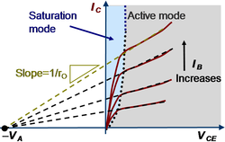
The figure shows two of the bipolar modes dividing a plot of transistor collector current versus collector-emitter voltage. The dividing curve is the current for VCE=VBE, or VCB=0. In words, this curve is the boundary between the collector collecting and the collector injecting. The saturation mode at low values of VCE is a region of strong current variation, while the active mode is a region of slow variation used in analog circuits. The inverse slope of the curves in the active region is the device output resistance, often approximated by the inverse slope of a fitted straight line that extrapolates to the device Early voltage, a performance parameter of the device. More detail is found in the article Bipolar transistor.
MOSFET
| MOS transistor | G-S Bias |
G-D Bias |
S-B Bias |
D-B Bias |
Mode |
|---|---|---|---|---|---|
| Channel at source end only | ≥ VT(S) | ≤ VT(D) | Zero or Reverse | More reverse than S-B | Active (Saturation) |
| Channel at both ends | ≥ VT(S) | > VT(D) | Zero or Reverse | More reverse than S-B | Ohmic (Triode)[1] |
| No channel | < VT(S) | < VT(D) | Zero or Reverse | Zero or reverse | Cutoff (Subthreshold) |
In the MOSFET, the threshold at source (or drain) is altered by the source-to-body (or drain-to-body) voltage, requiring a larger gate-to-source (gate-to-drain) voltage for channel formation the larger the reverse bias. Hence, the two threshold voltages VT(S) and VT(D) are different if the two reverse biases differ.
The term "cutoff" seems to imply no current flow at all, so for the MOSFET the term "subthreshold" sometimes is preferred. In subthreshold operation the current in the MOSFET decreases to very low values exponentially with gate voltage, and has very weak dependence upon drain-to-source voltage.
The table separates modes based upon the presence or absence of an inversion layer, or channel, at one or both ends of the channel region, concepts that retain meaning even for modern MOSFETs with very small dimensions and/or four-terminal operation. On the other hand, the obsolete Shichman-Hodges model that short-circuits the source to the body to obtain a three-terminal representation, bases the distinction between modes upon voltages: VDS < ( VGS – VT ) or VDS > ( VGS – VT ), a more limited approach.
In the MOSFET, the source and drain are interchangeable, so reverse operation simply exchanges the source for the drain. An exception is the power MOSFET, which like the bipolar transistor, has source and drain separately optimized for their particular function.
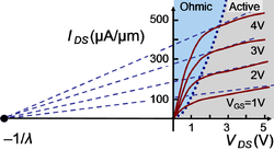
The figure shows two of the MOSFET modes dividing a plot of transistor drain current versus drain-source voltage. The body is short-circuited to the source. The boundary curve is the line VGD = VT (where V T is the threshold voltage for channel formation). In words, this curve is the current at a drain voltage high enough to extinguish the channel near the drain. The ohmic or triode mode at low values of VDS is a region of strong current variation, while the active or saturation mode is a region of slow variation used in analog circuits. The inverse slope of the curves in the active region is the device output resistance, often approximated by the inverse slope of a fitted straight line that extrapolates to the device Early voltage, a performance parameter of the device. In MOSFETs, the Early voltage VA usually is replaced by VA=1/λ, where λ is called the channel-length modulation parameter. More detail is found in the article MOSFET.
"On" and "off " modes
The use of on- and off-modes is illustrated with the bipolar inverter circuit shown at left. The circuit switches between "on" and "off" states (digital "one" and "zero") as the input VIN switches from "zero" to "one". That is, the output is the inverse of the input. The way things work is described next.
The input is shown as a switch that can toggle between ground (a "zero" input) and some nonzero voltage (a "one" input). The "one" input position is shown in the figure. It applies voltage VB to the base of the bipolar transistor, making the base-emitter voltage of this transistor VBE=VB. The value of VB is large enough to cause a large collector current IC to flow through the resistor, which causes a large voltage drop across the resistor according to Ohm's law. Consequently, the output voltage VOUT = VCC−ICRC is very low making the collector-emitter voltage VCE=VOUT so small that the transistor is driven into saturation mode. Thus, the "on" mode corresponds to the saturation mode of the transistor. The collector-emitter voltage when the transistor is in saturation often is designated by VCE(sat). This low output voltage is the "zero" level for the inverter output.
If now the switch is flipped to the ground position, the input is VIN=0 V. The transistor VBE is 0 V, and no collector current flows. Consequently the voltage drop across the resistor is zero, and VOUT=VCC, the supply voltage and the voltage corresponding to digital "one" for the inverter. The transistor is now in the "off" mode which corresponds to the cutoff mode.
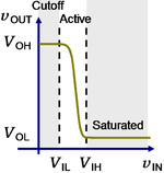
In practice, the input is not a switch, but a voltage signal, say vIN. As vIN is increased continuously from zero volts, the output voltage vOUT follows a transfer curve, as shown in the figure at right. The voltages corresponding to a digital "zero" or digital "one" are not precisely 0 V or VCC. The range of input voltages corresponding to a zero lie between 0 V and VIL, and corresponds to a digital "one" output voltageVOH. Likewise, a range of input voltages correspond to digital "one" voltages lies between VIH and VCC and results in a digital "zero" corresponding to VOL. If one inverter is used to drive another, output VOL serves as input to another inverter, and to work VOL≤VIL; likewise VOH≥VIH.
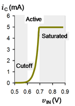
The "on" mode always corresponds to saturation, but strictly speaking the "off" mode does not cut off unless the circuit is somewhat modified from that shown, because the bipolar VBE for the circuit presented is nonzero and positive for positive vIN. That means strictly speaking the transistor is in active mode. As indicated in the figure illustrating the current for this application, however, the current is so low for small vIN that by convention the transistor nonetheless is described as being in cutoff.
A parallel discussion applies when the transistor is a MOSFET instead of a bipolar transistor. The body is short-circuited to the source and vIN = vGS. The MOSFET switches from the subthreshold or cutoff mode at low vIN, transiting the active mode, and ending up in the ohmic or triode mode at large vIN.
Amplifier operation
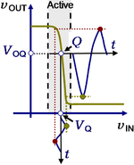
Input and output signals for bipolar inverter used as an electronic amplifier.
The role of transistor modes in electronic amplification is illustrated by use of the inverter as a signal amplifier. This amplifier is a form of common emitter amplifier (when a bipolar transistor is used) or of a common source amplifier (when a MOSFET is used), so-named after the transistor lead that is common to both the input (signal) side of the amplifier and to the output side.
To use the inverter as an analog amplifier, a DC bias is arranged that places the transistor in the active region of the transfer curve. The voltage vIN then becomes:
with VQ the quiescent or steady value of input voltage and vS the superposed signal. In the figure, the quiescent output is labeled VOQ and the Q-point as Q.
The input signal in the figure is indicated as a function of time. The output signal is constructed at a given time by determining for each input signal value the corresponding output voltage on the transfer curve using a vertical line. This value is then located at the corresponding time for the output voltage using a horizontal line. As can be seen from the steep transfer curve in the active region, the output of the inverter then consists of a very much amplified and inverted signal superposed upon the quiescent output voltage VOQ.
It can be seen that for large amplitude signals vS the input will hit the limits of the active region, crossing VIL or VIH and causing a flattening of the output signal at a value VOH or VOL, a distortion called clipping. Clipping is therefore a result of leaving the active mode and entering the saturation or the cutoff modes. It also may be seen that a faithful or undistorted output signal depends upon linearity of the transfer curve in the active region. The challenges for the analog designer are then (i) to arrange a good Q-point for the circuit, (ii) to arrange for a transfer curve with good linearity, (iii) to arrange for a width of the active region portion of the transfer curve that will avoid clipping at the required signal amplitude, and (iv) to arrange for the largest gain possible (a steep transfer curve). These goals cannot be simultaneously maximized, so trade-offs have to be introduced. For example, a steep transfer curve implies a narrow active region, which in turn requires a very stable biasing of the Q-point and very small-amplitude input signals.
References and notes
- ↑ The ohmic region sometimes is divided into the linear and the nonlinear ohmic regions, which jointly sometimes are called the "triode region". See Muhammad H. Rashid (2010). “§7.3.1 Operation: Linear ohmic region”, Microelectronic Circuits: Analysis and Design, 2nd ed. Cengage Learning, pp. 339 ff. ISBN 0495667722.
