Metal-oxide-semiconductor field-effect transistor
The Metal Oxide Semiconductor Field Effect Transistor (MOSFET) is a type of FET that consists of three layers: semiconductor (called body), oxide (working as insulator) and metal top electrode (conductor, called gate). This transistor was invented by Dawon Khang and Martin Atalla in 1960, at Bell Labs.[1]
There are four contacts altogether: in addition to the gate and body contacts already descirbed, there are two contacts atop the body at opposite sides of the gate called source and drain. Because the transistor is symmetrical, they can swap their functions. They do not permit current flow to the body in normal operation, as they form reverse biased diodes with the body. They do allow current between source and drain upon formation (by the gate) of a surface channel at the top surface of the body, next to the insulator. The channel conductivity depends upon the voltage difference between the gate and body (Vgb). The amount of current drawn in the channel depends upon the voltage drop across it, the drain to source voltage (Vds). The channel strength also is affected by so-called "back gate bias", that is, by the body to source voltage (Vbs).
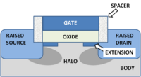
The modern MOSFET structure is shown in the figure. It is rather complex, as it is made to control a number of undesirable or parasitic effects that detract from its ideal behavior. Among these are unwanted capacitances between the gate and source and gate and drain, reduced by introduction of spacers at the sides of the gate. Another problem is high source-to-body and drain-to-body capacitance, which is reduced by raising the source and drain above the body, so the sidewall contact areas are reduced. These parasitic capacitances have to be charged and discharged between on and off conditions, and slow down device operation. Also undesired is penetration of the source and drain fields underneath the gate, which interferes with the channel formation. That effect is reduced by use of shallow junction extensions and screening halo implants, both designed to keep the source and drain fields close to their electrodes, and away from the gate.
Channel formation
A narrow, surface inversion layer of electrons forms at large enough positive gate voltages. The horizontal dashed line indicates the Fermi level that divides occupied energy levels from empty ones at zero temperature.
The control of the channel by the gate is similar to the formation of an inversion layer in the MOS Capacitor, which is only a two-terminal device (gate and body contacts). The case of a p-type semiconductor body in which mobile holes are introduced in the valence band by introducing acceptor impurities is described below. The acceptors suck electrons out of the valence band, becoming fixed negative ions, and leaving electron vacancies in the valence band that behave as positively charge mobile holes.
The formation of this layer is understood by examining the behavior of the energy band edges under an applied field. The left-hand panels of the figure depict the lowest energy level of the conduction band of energies and the highest energy level of the valence band of energies (separated by the forbidden gap with no available energy levels) as a function of depth into the semiconductor body. In the figure's top panel, an applied voltage bends these band edges (left). This bending causes the valence band to become filled with electrons, so no holes are present. On the upper right, the figure shows the charge inducing this bending (Q) is balanced by a layer of negative acceptor-ion charge –QA in this depletion region where there are no holes. This depletion region of negative acceptor ions widens until neutrality is reached Q−QA = 0. In the bottom panel, a larger applied voltage further depletes holes from the surface but the conduction band becomes low enough in energy to populate with electrons near the surface, forming an inversion layer. The charge inducing the inversion layer is now balanced both by the inversion layer charge –Qn and by the depletion layer charge –QA, so now Q–Qn−QA = 0. Once the applied voltage is large enough to begin formation of the inversion layer, the charge balance is dominated by this layer, and the depletion region no longer expands significantly.
The electrons in the surface channel are mobile and form a conducting surface layer atop the insulating layer of fixed, immobile acceptor ions in the depletion region. The source and drain contacts on the body surface become connected by this conducting surface layer, so the formation of the inversion layer allows current to flow from the source to the drain. By contrast, when the conducting surface layer is not present, no conduction occurs, even when the surface layer is not depleted and holes are present. The contacts cannot conduct using holes because they are n-type semiconductor regions, and form pn-diode junctions with the body.
Thus, the source and drain are not electrically connected for voltages between zero and the threshold voltage for inversion layer formation. But once threshold voltage is exceeded, connection is established. The MOSFET constitutes an electrically controlled switch.
Notes
- ↑ An historical run-down with references can be found in Gianfranco Cerofolini (2009). “Chapter 2: Top-down paradigm to miniaturization”, Nanoscale Devices: Fabrication, Functionalization, and Accessibility from the Macroscopic World. Springer, pp. 9 ff. ISBN 354092731X.
