Fermi function
Fermi function
The Fermi function or, more completely, the Fermi-Dirac distribution function describes the occupancy of a electronic energy level in a system of electrons at equilibrium. The occupancy f(E) of an energy level of energy E at an absolute temperature T in kelvins is given by:
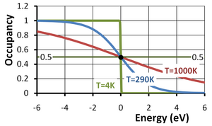
Here EF is called the Fermi energy and kB is the Boltzmann constant. This occupancy function is plotted in the figure versus the energy E−EF in eV (electron volts). In the second form of the function above, the energy is in eV (that is, in the form E/q) and the temperature appears as the thermal voltage kBT/q (approximately 25 mV at 290K). As temperature increases, so does the thermal voltage, accounting for the stretching out of the function along the energy axis with increasing temperature.
Notice that for an energy level with E = EF and a degeneracy factor g = 1 (see below for a discussion of g), the occupancy is 1/2 regardless of temperature. The Fermi level EF thus can be referred to as the half-occupancy level.
Boltzmann limit
For energy levels such that the exponential in the Fermi function becomes large compared to 1, the Fermi function can be approximated by this exponential alone as:
On this basis the relative population of an energy E1 compared to one of energy E2 is:
which is the form derived using Maxwell-Boltzmann statistics, a classical approach based upon a gas of point particles exchanging energy by collisions to achieve thermal equilibrium.
Dopant levels
Dopant impurities are used in semiconductors to adjust the conductivity of the material. They introduce energy levels for electrons, usually in the energy gap between the conduction and valence band edges. If the impurities are acceptors, these levels are close to the valence band edge and become negatively charged when occupied. If they are donor impurities, the levels are introduced near the conduction band edge, and when vacated lead to localized positive charges.
Some impurities (or crystal defects) introduce "deep levels" closer to the middle of the gap and these can be charge-ambivalent: they can have either sign of charge or be neutral. Such mid-gap energy levels may serve as recombination-generation centers, assisting in generation or recombination of holes and electrons. They often are called Shockley-Reed-Hall centers.[1]
Suppose energies are measured from the valence band edge in a semiconductor, so the impurity energy level becomes Ea,d = E−EV and EF is replaced by EF − EV. Then the occupancy of the impurity level is given by:
where g is the so-called degeneracy factor. The origin of the degeneracy factor goes back to the underlying derivation of the Fermi function, which is fundamentally a determination of the most probable way n-electrons can be distributed among N energy levels while constrained by a fixed energy for the ensemble.[2] In this counting of permutations, the contribution of the impurities is included by making some basic assumptions about the impurity behavior that are essentially empirical in nature. For example, one may postulate that the impurity atoms divide into two populations, one with ni electrons and the other with ni+1 electrons. Moreover, we suppose that the electrons on any one atom in the first population may fall into any of g0 possible equivalent levels, while for those in the second population there are g1 possible levels. Then the degeneracy factor in the Fermi occupancy function is found to be g0/g1.[3] [4]
Typically an acceptor provides an energy level related to the valence band structure of the host material. A common case is two valence bands: a "heavy" hole valence band and a "light" hole valence band, either of which may populate the acceptor. Thus, the number of negatively charge acceptors, compared to the total number of acceptors, is:
where the degeneracy factor of 4 stems from the possibility of either a spin-up or a spin-down electron occupying the level Ea, and the existence of two sources for holes of energy Ea, one from the "heavy" hole band and one from the "light" hole band.
In contrast to acceptors, donors become positively charged and tend to give up an electron. The number of positive donors compared to the total number of donors is then:
where now the degeneracy factor is 2 (because of the spin-up or spin-down possibilities for occupancy) and there is typically only one conduction band associated with the energy level Ed.[5]
Fermi level
The Fermi level or Fermi energy, EF, in the Fermi function represents for a system of independent electrons a very special case of the more general notion of an electrochemical potential. The chemical potential of a chemical species is the work required to add a particle of that species to an ensemble of particles at constant temperature and pressure. The electrochemical potential is the same quantity, but for a charged particle that has both chemical and electrical interactions.[6]
For a system of independent electrons, this energy is the Fermi energy. Based upon the interpretation as the work necessary to add a particle to an ensemble of particles, the Fermi level in a system at thermal equilibrium must be the same at every point in the system. If that were not so, the system would change its overall energy by moving a particle from one location to another, contradicting the assumption of equilibrium.
Locating the Fermi level
If a material has a density of states D(E) that determines how many energy levels lie in the infinitesimal interval dE centered at energy E, then the number of electrons N in the system is given by:
which determines the position of the Fermi level EF in terms of the number of electrons N.
For example, in a semiconductor, the Fermi level lies in the energy gap between the valence band and the conduction band. For a semiconductor with a positively charged donor impurity density N+D the number of electrons in the conduction band alone is approximately the same as the number of charged donors. Taking the density of states in the conduction band as D(E) with E measured from the conduction band edge at EC, this equality results in:
The approximate Boltzmann form of the Fermi function is introduced. The energy integral is usually called the "effective density of states" of the conduction band and denoted as NC. Then:
The density of states is considerably larger than the density of impurities, so the logarithm is negative, placing the Fermi level below the conduction band edge. Assuming the density of states in this integral can be approximated by a simple parabolic energy-wavevector relation in MC equivalent valleys,[7]
the effective density of states is:
In a similar fashion, the Fermi level in a semiconductor containing negative acceptors is determined to lie just above the valence band edge.
Built-in potentials
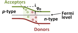
As a consequence of the Fermi level representing the work done in addition of an electron, built-in potentials or contact potentials arise in joining inhomogeneous materials, for example, in pn-junctions. In this case, the Fermi level on the p-type side is positioned in energy near the valence band edge, reducing the electron occupancy of the valence band and thereby increasing the hole density, as expected for p-type material. On the n-type side, it is positioned near the conduction band edge, which makes the electron density high, as appropriate to n-type material. If these two materials are joined and electrons are allowed to flow freely between the two sides, equilibrium results when the work done in placing an electron on the p-side is the same as that done placing an electron on the n-side; that is, equilibrium requires the Fermi levels on the two sides must be the same. If that were not so, a current would flow in a wire joining the two sides, contradicting the notion of equilibrium.
As the figure shows, the flat Fermi level implies the band edges on the p-type side are shifted in energy compared to the n-type side. The potential energy difference is the difference in energy (expressed in eV) on the two sides between (say) the valence band edge and the Fermi level on each side. From an electrostatic point of view, this potential difference is correlated with a so-called double layer of charged ions, negative acceptor ions on the p-side and positive donor ions on the n-side. According to the Poisson equation, this charge leads to a potential. The amount of charge of each type is the same, because the widths of the negative ion region and the positive ion region adjust to make this true, so the bulk semiconductor on either side exhibits zero field and the potential is constant in the bulk materials.
Quasi-Fermi levels (IMREFs)
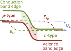
The notion of Fermi energy or Fermi level applies to a system in thermal equilibrium. In cases where an electric current flows under an applied voltage, the system is not in thermal equilibrium, but the occupancy of energy levels is sometimes described in such cases using quasi-Fermi levels, or imrefs (Fermi spelled backward). The figure shows a typical example of this usage, namely the reverse-biased pn-junction (see Semiconductor diode). The reverse bias raises the equilibrium Fermi level on the p-type side above that on the n-type side by the applied reverse bias value VR. Here the electron occupancy is described by the electron quasi-Fermi level EFn that indicates the neutral bulk equilibrium Fermi level for electrons continues into the p-type region for a significant distance before collapsing to the equilibrium hole Fermi level in the p-type bulk. That means that the electron density is significantly reduced from its value on the n-type side, as indicated by the conduction band edge bending away from the quasi-Fermi level, and on the p-type side is much lower in the transition region than it is in the neutral bulk p-type material. Deep in the p-type region, the electron quasi-Fermi level rejoins the neutral bulk equilibrium Fermi level, and holes and electrons have the same equilibrium Fermi level. A similar description applies to the hole quasi-Fermi level EFp with the roles of p-type and n-type interchanged.[8] Of course, a leakage current flows in the reverse biased junction, so the bulk regions are not strictly at equilibrium, and the notion that the equilibrium Fermi levels apply in the neutral bulk is an approximation.
Fermi surface
At zero temperature, the energy levels up to the Fermi energy are full, and those below are empty. For an assembly of particles occupying these energy levels, the equation E = EF defines a surface in the space of parameters determining the energy, such as the particle momentum. This surface, separating the filled from the empty energy levels, is called the Fermi surface.
For example, for an ideal "gas" of independent electrons, the energy of an electron in the gas is given by:
where m is the electron mass, and the wavevector k is related to momentum p by p = ћk, where ћ is Planck's constant divided by 2π. The wavevector is related to the de Boglie wavelength of the particle.
For this ideal electron gas, the equation E = EF defines a spherical surface in the space of the wavevector. The energy of an electron in a solid is a more complicated function of the wavevector k. The figure shows a possible Fermi surface in a face-centered cubic lattice, as contained inside the Brillouin zone for this lattice, a volume in k-space that bounds the values of k corresponding to distinct energies.[9] As may be seen, far from being spherical, in a crystal the Fermi surface can be complex indeed.
Notes
- ↑ Graham T. Reed (2008). “§6.2.2 Recombination and generation via deep levels”, Silicon photonics: the state of the art. Wiley, pp. 193 ff. ISBN 0470025794.
- ↑ The most probable way to populate the available energy levels is found by counting how many ways electrons can be arranged in the various levels consistent with the given total energy and total number of electrons, and picking the configuration that corresponds to the most numerous ways to achieve it. So, for example, for electrons in a featureless box, a configuration with all the electrons located in a corner of their container is found to be achieved in vastly fewer ways than a configuration with the electrons spread out over the entire region available. Consequently, the equilibrium case is the delocalized rather than the localized configuration. Inhomogeneous fluctuations about the most probable case do occur, but they are fleeting. See, for example, Kevin F. Brennan (1999). The physics of semiconductors: with applications to optoelectronic devices. Cambridge University Press. ISBN 0521596629.
- ↑ Such a derivation can be found in David C. Look (1983). “Chapter 2: Properties of semi-insulating GaAs: Appendix B”, Robert K. Willardson, Albert C. Beer: Deep levels, GaAs, alloys, photochemistry; volume 19 of Semiconductors and Semimetals. Academic Press, pp. 149 ff. ISBN 0127521194.
- ↑ K Seeger (2004). “§3.2 Occupation probabilities of impurity levels”, Semiconductor physics: An introduction, 9th ed. Springer, pp. 41 ff. ISBN 3540219579.
- ↑ Michael Reisch (2003). “§2.2.2 Ionization”, High-frequency bipolar transistors: physics, modelling, applications. Springer. ISBN 354067702X.
- ↑ See, for example, Wolfgang Schmickler (1996). “§2.2 The electrochemical potential”, Interfacial electrochemistry. Oxford University Press, pp. 13 ff. ISBN 0195089324.
- ↑ SM Sze and KK Ng (2007). Physics of semiconductor devices, 3rd ed. Wiley, p. 17. ISBN 0471143235.
- ↑ See, for example, the previously cited book by K. Seeger. “§5.4 Quasi-Fermi levels”, Semiconductor physics: An introduction, pp.135 ff. ISBN 3540219579.
- ↑ For values of k outside the Brillouin zone, the energy repeats itself periodically. A rather complete introduction is found in Richard H. Bube (1992). Electrons in solids: an introductory survey, 3rd ed. Academic Press, p. 119, Figure 7.5. ISBN 0121385531.


