User:John R. Brews/Draft
Schottky diode
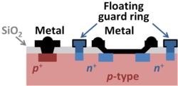
The Schottky diode is a two-terminal device consisting of conductive gate (for example, a metal) on top of a semiconductor body. A generic name for this structure is the metal-semiconductor diode or M/S diode.[1] For low voltage applications, below 200V, silicon is used, but for higher voltages (up to 3000 V or more) silicon carbide is used to extend the breakdown voltage. These voltages are achievable only when edge breakdown is avoided, which requires special attention to edge termination designs.[2] The figure shows three strategies toward increasing the edge breakdown voltage: an extension of the metal diode contact over a tapered oxide and also an n+-guard ring and a floating metal guard ring. These strategies are sometimes used together, but also are used separately. The substrate contact is made through an ohmic contact to the p-substrate made using a metal-to-p+ region on the surface of the diode.
Notes
- ↑ The term "Schottky diode" may be taken erroneously to refer to diffusion as the mechanism of operation as first proposed by Mott, Schottky and Davydov. However, the mechanism in most devices is thermionic emission, as later proposed by Bethe. See Chih-Tang Sah (1991). “§560: Metal/semiconductor diode”, Fundamentals of solid-state electronics. World Scientific, p. 474. ISBN 9810206372.
- ↑ B. Jayant Baliga (2005). “§3.2 Schottky diode edge terminations”, Silicon carbide power devices. World Scientific, pp. 44 ff. ISBN 9812566058.
http://books.google.com/books?id=FPlJQ0iO7oQC&pg=PA134&dq="Schottky+diode"&hl=en&ei=iAg6TeO7AYSasAOk67WhAw&sa=X&oi=book_result&ct=result&resnum=8&ved=0CGIQ6AEwBw#v=onepage&q="Schottky diode"&f=false
