imported>John R. Brews |
imported>John R. Brews |
| Line 58: |
Line 58: |
| |Silicon conduction band ellipsoids.JPG|A constant energy surface in the silicon conduction band consists of six ellipsoids. | | |Silicon conduction band ellipsoids.JPG|A constant energy surface in the silicon conduction band consists of six ellipsoids. |
| |Planar Schottky diode.PNG|Planar Schottky diode with ''n<sup>+</sup>''-guard rings and tapered oxide. | | |Planar Schottky diode.PNG|Planar Schottky diode with ''n<sup>+</sup>''-guard rings and tapered oxide. |
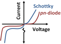
| | |Schottky & pn diode IV curves.PNG|Comparison of Schottky and ''pn''-diode current voltage curves. |
| | |Schottky barrier height.PNG|Schottky barrier formation on ''p''-type semiconductor. Energies are in eV. |
| | |Schottky barrier (forward bias).PNG|Under forward bias ''V<sub>F</sub>'' the Schottky barrier height is reduced and the Fermi levels are split. |
| | |Schottky barrier (reverse bias).PNG|Schottky diode under reverse bias ''V<sub>R</sub>''. |
| }} | | }} |
Revision as of 17:00, 1 February 2011
I am a Professor Emeritus of Electrical Engineering from The University of Arizona, where I taught device physics and circuit design for just under two decades. Previously, I was a research scientist for twenty-odd years at Bell Laboratories, Murray Hill, doing theoretical work in the areas of solid-state physics and device physics. I also am a Fellow of the IEEE, and a recipient of the Electron Device Society distinguished service award for work as Editor-in-chief of the journal IEEE Electron Device Letters, founded by Nobel prize winner George E. Smith. I've published a number of technical books and papers, some of which may be found at this link.
Images
| Magnetism
|
|
|
(CC) Image: John R. Brews
|
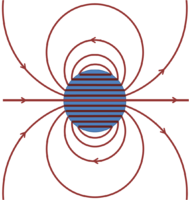
B-field lines near uniformly magnetized sphere
|
|
|
(CC) Image: John R. Brews
|
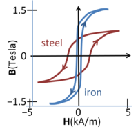
Magnetic flux density vs. magnetic field in steel and iron
|
|
| Widlar current source
|
|
|
(CC) Image: John R. Brews
|
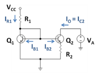
Widlar current source using bipolar transistors
|
|
|
(CC) Image: John R. Brews
|
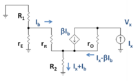
Small-signal circuit for finding output resistance of the Widlar source
|
|
|
(CC) Image: John R. Brews
|
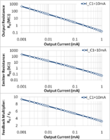
Design trade-off between output resistance and output current in Widlar source
|
|
| Forces
|
|
|
(CC) Image: John R. Brews
|
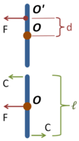
Force and its equivalent force and couple
|
|
| Electromagnetism
|
|
|
(CC) Image: John R. Brews
|
|
|
|
| Devices
|
|
|
(PD) Image: John R. Brews
|
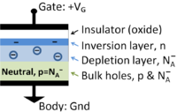
Cross section of MOS capacitor showing charge layers
|
|
|
(PD) Image: John R. Brews
|
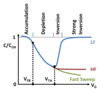
Three types of MOS capacitance vs. voltage curves. VTH = threshold, VFB = flatbands
|
|
|
(PD) Image: John R. Brews
|
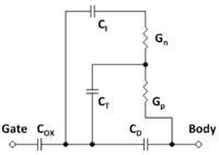
Small-signal equivalent circuit of the MOS capacitor in inversion with a single trap level
|
|
|
(PD) Image: John R. Brews
|
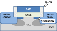
A modern MOSFET
|
|
|
(PD) Image: John R. Brews
|
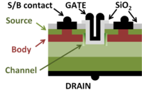
A power MOSFET; source and body share a contact.
|
|
|
(CC) Image: John R. Brews
|
Calculated density of states for crystalline silicon.
|
|
|
(CC) Image: John R. Brews
|
Field effect: At a gate voltage above threshold a surface inversion layer of electrons forms at a semiconductor surface.
|
|
|
(PD) Image: John R. Brews
|
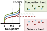
Occupancy comparison between n-type, intrinsic and p-type semiconductors.
|
|
|
(PD) Image: John R. Brews
|
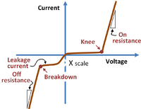
Nonideal pn-diode current-voltage characteristics
|
|
|
(PD) Image: John R. Brews
|
Band-bending diagram for pn-junction diode at zero applied voltage
|
|
|
(PD) Image: John R. Brews
|
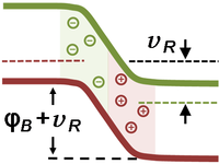
Band-bending for pn-diode in reverse bias
|
|
|
(PD) Image: John R. Brews
|
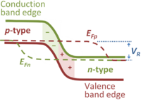
Quasi-Fermi levels in reverse-biased pn-junction diode
|
|
|
(PD) Image: John R. Brews
|
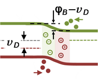
Band-bending diagram for pn-diode in forward bias
|
|
|
(PD) Image: John R. Brews
|
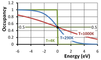
Fermi occupancy function vs. energy departure from Fermi level in volts for three temperatures
|
|
|
(PD) Image: John R. Brews
|
Fermi surface in k-space for a nearly filled band in the face-centered cubic lattice
|
|
|
(PD) Image: John R. Brews
|
A constant energy surface in the silicon conduction band consists of six ellipsoids.
|
|
|
(PD) Image: John R. Brews
|
Planar Schottky diode with n+-guard rings and tapered oxide.
|
|
|
(PD) Image: John R. Brews
|
Comparison of Schottky and pn-diode current voltage curves.
|
|
|
(PD) Image: John R. Brews
|
Schottky barrier formation on p-type semiconductor. Energies are in eV.
|
|
|
(PD) Image: John R. Brews
|
Under forward bias VF the Schottky barrier height is reduced and the Fermi levels are split.
|
|
|
(PD) Image: John R. Brews
|
Schottky diode under reverse bias VR.
|
|
