User:John R. Brews/Images: Difference between revisions

From Citizendium
Jump to navigation Jump to search
imported>John R. Brews
No edit summary
No edit summary
 
(59 intermediate revisions by one other user not shown)
Line 1: Line 1:
{{AccountNotLive}}
{{DEFAULTSORT:Brews, John R.}}
{{TOC|right}}
{{TOC|right}}
Angle brackets:  & #x27E8; <nowiki>=</nowiki> &#x27E8; &emsp;  & #x27E9; <nowiki>=</nowiki> &#x27E9; &emsp;  & #10216; <nowiki>=</nowiki> &#10216; &emsp;  & #10217;<nowiki>=</nowiki> &#10217;
Angle brackets:  & #x27E8; <nowiki>=</nowiki> &#x27E8; &emsp;  & #x27E9; <nowiki>=</nowiki> &#x27E9; &emsp;  & #10216; <nowiki>=</nowiki> &#10216; &emsp;  & #10217;<nowiki>=</nowiki> &#10217; <nowiki><Φ|Ψ></nowiki> <Φ|Ψ> <big><nowiki><</nowiki></big>Φ|Ψ<big><nowiki>></nowiki></big> &#x27E8;Φ|Ψ&#x27E9; &#10216;Φ|Ψ&#10217; <math>\langle \Phi|\Psi \rangle </math> &lang;Φ|Ψ&rang; '''&lang;'''Φ|Ψ'''&rang;'''
==Photos==
==Photos==
{{Gallery-mixed
{{Gallery-mixed
|caption=Photos
|caption=Photos  
|width=200
|width=200
|lines=5
|lines=5
|Mourning dove nest.JPG|Mourning dove on nest in Tucson
|Mourning dove nest.JPG|Mourning dove on nest in Tucson
|Mourning dove and squab.JPG|Morning dove with squab, Tucson AZ.
|Dove with squab.JPG|Mourning dove with squab.
|Mourning dove squab.JPG|Mourning dove squab.
|Dove on saguaro.JPG|Mourning dove on saguaro cactus, Tucson AZ.
}}
}}
==Magnetism==
==Magnetism==
{{Gallery-mixed
{{Gallery-mixed
Line 16: Line 22:
|Magnetized sphere.PNG|'''B'''-field lines near uniformly magnetized sphere
|Magnetized sphere.PNG|'''B'''-field lines near uniformly magnetized sphere
|Hysteresis loops.PNG|Magnetic flux density ''vs.'' magnetic field in steel and iron
|Hysteresis loops.PNG|Magnetic flux density ''vs.'' magnetic field in steel and iron
|Parallel wires.PNG|'''''B'''''-field from current '''''I<sub>2</sub>''''' in wire ''2'' causes force '''''F''''' on wire ''1''.
}}
}}
==Chemistry==
{{Gallery-mixed
|caption=Chemistry
|width=200
|lines=5
|Reaction path.PNG|Reactants cross an energy barrier, enter an [[Transition state|intermediate state]] and finally emerge in a lower energy configuration.
}}
==Circuits==
==Circuits==
{{Gallery-mixed
{{Gallery-mixed
|caption=Widlar current source
|caption=Current sources
|width=200
|width=200
|lines=5
|lines=5
Line 25: Line 41:
|Widlar small-signal.PNG|Small-signal circuit for finding output resistance of the Widlar source
|Widlar small-signal.PNG|Small-signal circuit for finding output resistance of the Widlar source
|Widlar Resistance Plot.PNG|Design trade-off between output resistance and output current in Widlar source
|Widlar Resistance Plot.PNG|Design trade-off between output resistance and output current in Widlar source
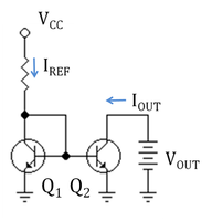
|Simple bipolar mirror.PNG|A current mirror implemented with npn bipolar transistors using a resistor to set the reference current I<sub>REF</sub>; V<sub>CC</sub><nowiki> = </nowiki>supply voltage.
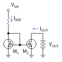
|Simple MOSFET mirror.PNG| An n-channel MOSFET current mirror with a resistor to set the reference current
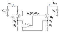
|Gain-assisted current mirror.PNG| Gain-boosted current mirror with op amp feedback to increase output resistance.
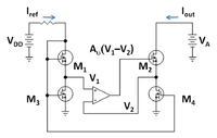
|Wide-swing MOSFET mirror.PNG| MOSFET version of wide-swing current mirror; M<sub>1</sub> and M<sub>2</sub> are in active mode
|Current sink.PNG|Operational-amplifier based current sink. Because the op amp is modeled as a nullor, op amp input variables are zero regardless of the values for its output variables.
|Bipolar inverter.PNG|A digital inverter circuit using a bipolar transistor.
|Transfer characteristic of bipolar inverter.PNG|Transfer characteristic of bipolar inverter showing modes.
|Current in bipolar inverter.PNG|Collector current ''vs.'' input voltage for a bipolar inverter with ''V<sub>CC</sub>''<nowiki>=</nowiki>5V and ''R<sub>C</sub>''<nowiki>=</nowiki>1k&Omega;.
|Amplifier input and output.PNG|Input and output signals for bipolar inverter used as an amplifier.
|Two-port with Thevenin driver.PNG| Two-port network with symbol definitions.
|Z-equivalent two-port.PNG| Z-equivalent two port showing independent variables ''I<sub>1</sub>'' and ''I<sub>2</sub>''.
|Y-equivalent two-port.PNG| Y-equivalent two port showing independent variables
|H-equivalent two-port.PNG|H-equivalent two-port showing independent variables
|G-equivalent two-port.PNG| G-equivalent two-port showing independent variables
|Block diagram asymptotic gain.PNG|Block diagram for asymptotic gain model
|Signal-flow graph for asymptotic gain model.PNG|Possible signal-flow graph for the asymptotic gain model
|MOSFET Transresistance amplifier.PNG| MOSFET transresistance feedback amplifier.
|Bipolar transresistance feedback amplifier.PNG| Collector-to-base biased bipolar amplifier.
|Shunt-series feedback amplifier.PNG|Two-transistor feedback amplifier; any source impedance ''R<sub>S</sub>'' is lumped in with the base resistor ''R<sub>B</sub>''.
}}
}}
{{Gallery-mixed
|caption=Small-signal circuits
|width=200
|lines=5
|PN-diode small-signal circuit2.PNG|Small-signal circuit for ''pn-''diode driven by a current signal represented as a [[Norton's theorem|Norton source]].
|Bipolar current mirror with emitter resistors.PNG| Bipolar current mirror with emitter resistors
|Small-signal circuit for bipolar mirror.PNG| Small-signal circuit for bipolar current mirror
|Common base with current drive.PNG| Common base circuit with active load and current drive.
|Common base with current driver.PNG|Common-base amplifier with AC current source ''I<sub>1</sub>'' as signal input
|Common base with voltage drive.PNG|Bipolar transistor with base grounded and signal applied to emitter.
|Small-signal common base circuit.PNG|Common-base amplifier with AC voltage source ''V<sub>1</sub>'' as signal input
|Norton equivalent circuit.PNG|The result of applying Norton's theorem.
|Current follower.PNG|Bipolar current buffer.
|Current follower; small-signal.PNG|Small-signal circuit to find output current.
|Current follower output resistance.PNG|Small-signal circuit with test current ''i<sub>X</sub>'' to find Norton resistance.
|Thevenin equivalent circuit.PNG|The result of applying Thévenin's theorem.
|Voltage Follower.PNG|Bipolar buffer.
|Voltage Follower Small-signal.PNG|Small-signal circuit for voltage follower.
|Voltage follower output resistance.PNG|Determination of the small-signal output resistance.
|Bipolar hybrid-pi model.PNG| Simplified, low-frequency hybrid-pi [[BJT]] model.
|Bipolar hybrid-pi capacitances.PNG|Bipolar hybrid-pi model with parasitic capacitances.
|Bipolar hybrid-pi model.PNG| Simplified, low-frequency hybrid-pi [[BJT]] model.
|Bipolar hybrid-pi capacitances.PNG|Bipolar hybrid-pi model with parasitic capacitances.
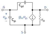
|MOSFET hybrid-pi with capactances.PNG|Simplified, three-terminal MOSFET hybrid-pi model.
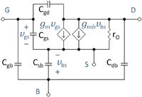
|MOSFET four-terminal hybrid-pi circuit.PNG|Four-terminal small-signal MOSFET circuit.
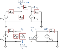
|Miller effect.PNG|Miller effect: These two circuits are equivalent.
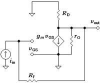
|Small-signal transresistance amplifier.PNG| Small-signal circuit for transresistance amplifier
|Return ratio.PNG|Small-signal circuit with return path broken and test current ''i<sub>t</sub>'' driving amplifier at the break.
|Using return ratio.PNG|Three small-signal schematics used to discuss the asymptotic gain model
}}
{{Gallery-mixed
|caption=Return ratio
|width=500
|lines=5
|Inserting source for return ratio.PNG|''Left'' - small-signal circuit corresponding to bipolar amplifier; ''Center'' - inserting independent source and marking leads to be cut; ''Right''  - cutting the dependent source free and short-circuiting broken leads.
}}
{{Gallery-mixed
|caption=Amplifiers
|width=200
|lines=5
|Aspects of step response.PNG|Some terms used to describe step response in time domain.
|Negative feedback amplifier.PNG|Ideal negative feedback model; open loop gain is ''A''<sub>OL</sub> and feedback factor is β.
|Conjugate poles.PNG|Conjugate pole locations for step response of two-pole feedback amplifier.
|Step response of negative feedback amplifier.PNG| Step-response of a linear two-pole feedback amplifier.
|Overshoot control.PNG|Step response for three values of time constant ratio.
|Gain Bode plot for two-pole amplifier.PNG|Bode gain plot to find phase margin of two-pole amplifier.
|High-pass amplifier Bode plot.PNG|The Bode plot for a first-order (one-pole) [[highpass filter]]
|Low-pass amplifier Bode plot.PNG|The Bode plot for a first-order (one-pole) [[lowpass filter]]
|Bode plot for pole and zero.PNG| Bode magnitude plot for zero and for low-pass pole
|Bode phase plot for pole and zero.PNG|Bode phase plot for zero and for low-pass pole
|Superposed Bode plots for pole and zero.PNG|Bode magnitude plot for pole-zero combination; the location of the zero is ten times higher than in above figures
|Superposed Bode phase plots for pole and zero.PNG|Bode phase plot for pole-zero combination; the location of the zero is ten times higher than in above figures
|Open and closed loop gain.PNG|Gain of feedback amplifier ''A''<sub>FB</sub> in dB and corresponding open-loop amplifier ''A''<sub>OL</sub>.
|Open and closed loop phase.PNG|Phase of feedback amplifier ''°A''<sub>FB</sub> in degrees and corresponding open-loop amplifier ''°A''<sub>OL</sub>.
|Gain margin.PNG|Gain of feedback amplifier ''A''<sub>FB</sub> in dB and corresponding open-loop amplifier ''A''<sub>OL</sub>.
|Phase margin.PNG|Phase of feedback amplifier ''A''<sub>FB</sub> in degrees and corresponding open-loop amplifier ''A''<sub>OL</sub>.
|Pole splitting example.PNG| Operational amplifier with compensation capacitor ''C<sub>C</sub>'' between input and output to cause pole splitting.
|Pole splitting with Miller transformation.PNG|Operational amplifier with compensation capacitor transformed using [[Miller effect|Miller's theorem]] to replace the compensation capacitor with a Miller capacitor at the input and a frequency-dependent current source at the output.
|Two-pole Bode magnitude plot.PNG|Idealized [[Bode plot]] for a two pole amplifier design.
|Compensation capacitance.PNG|Miller capacitance at low frequencies ''C<sub>M</sub>'' (top) and compensation capacitor ''C<sub>C</sub>'' (bottom) as a function of gain
}}
==Logic==
{{Gallery-mixed
|caption=Logic and Venn diagrams
|width=150
|lines=5
|Venn Diagrams.PNG|Venn diagrams; set A is the interior of the blue circle (left), set B is the interior of the red circle (right).
|Venn diagrams XY.PNG|Venn diagrams; set ''X'' is the interior of the blue circle (left), set ''Y'' is the interior of the red circle (right).
|Venn diagram for subsets of two sets.PNG|Venn diagram showing subsets of two sets ''X'' and ''Y''.
|Venn diagram for three sets.PNG|Venn diagram for three sets ''X'', ''Y'', and ''Z''.
|Venn diagram for four sets.PNG|Venn diagram for four sets ''X'', ''Y'', ''Z'', and ''W''.
|Venn diagram for five sets.PNG|Venn diagram for five sets ''X'', ''Y'', ''Z'', ''V'' and ''W''.
|Logic gate with Venn diagram.PNG|A three-input logic gate (center) with its Venn diagram (top) and truth table (bottom).
|Venn diagram for switch network A.PNG|Five-switch network with Venn diagrams for branches
|Venn diagram for switch network B.PNG|Equivalent three-switch network with Venn diagrams for branches
}}
==Forces==
==Forces==
{{Gallery-mixed
{{Gallery-mixed
Line 71: Line 188:
|Interferometer.PNG|Measuring a length using interference fringes.
|Interferometer.PNG|Measuring a length using interference fringes.
|Waves in a box.PNG|The wavelengths of standing waves in a box that have zero amplitude (nodes) at the walls.
|Waves in a box.PNG|The wavelengths of standing waves in a box that have zero amplitude (nodes) at the walls.
|Michelson interferometer.PNG|Measuring a length in wavelengths of light using a [[Michelson interferometer]].
|Doppler effect.PNG|Boat opposing incoming waves experiences the Doppler effect
|Doppler with moving source.PNG|Doppler shift with moving source
|Current elements.PNG|Infinitesimal current elements in two closed current-carrying loops
|Lienard-Wiechert coordinates.PNG|Origin at ''0'', observation point at ''P'', and present position of charge ''q'' distant by ''R'' from observation point ''P''.
}}
}}


Line 78: Line 200:
|width=200
|width=200
|lines=5
|lines=5
|Two diode structures.PNG|Mesa diode structure (top) and planar diode structure with guard-ring (bottom).
|Planar bipolar transistor.PNG|A planar bipolar junction transistor as might be constructed in a [[integrated circuit]].
|Gummel plot.PNG|Gummel plot and current gain for a GaAs/AlGaAs heterostructure bipolar transistor.
|Diode quasi-fermi levels.PNG|Quasi-Fermi levels and carrier densities in forward biased ''pn-''diode.
|MOS Capacitor.PNG|Cross section of MOS capacitor showing charge layers
|MOS Capacitor.PNG|Cross section of MOS capacitor showing charge layers
|MOS CV curves.PNG|Three types of MOS capacitance ''vs.'' voltage curves. ''V<sub>TH</sub>''&nbsp;<nowiki>=</nowiki>&nbsp;threshold, ''V<sub>FB</sub>''&nbsp;<nowiki>=</nowiki>&nbsp;flatbands&nbsp;
|MOS CV curves.PNG|Three types of MOS capacitance ''vs.'' voltage curves. ''V<sub>TH</sub>''&nbsp;<nowiki>=</nowiki>&nbsp;threshold, ''V<sub>FB</sub>''&nbsp;<nowiki>=</nowiki>&nbsp;flatbands&nbsp;
Line 83: Line 209:
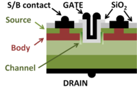
|MOSFET junction structure.PNG|A modern MOSFET  
|MOSFET junction structure.PNG|A modern MOSFET  
|UMOSFET.PNG|A power MOSFET; source and body share a contact.
|UMOSFET.PNG|A power MOSFET; source and body share a contact.
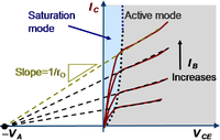
|Early effect.PNG|Two bipolar transistor modes, showing extrapolation of asymptotes to the Early voltage.
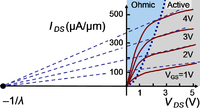
|Channel length modulation.PNG|Channel length modulation in 3/4&mu;m technology.
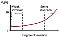
|Early voltage for 0.18mu process.PNG|Early voltage for MOSFETs from a 0.18&mu;m process as a function of channel strength.
|Silicon density of states.PNG|Calculated density of states for crystalline silicon.
|Silicon density of states.PNG|Calculated density of states for crystalline silicon.
|Seimiconductor band bending.PNG|''Field effect'': At a gate voltage above threshold a surface inversion layer of electrons forms at a semiconductor surface.
|Seimiconductor band bending.PNG|''Field effect'': At a gate voltage above threshold a surface inversion layer of electrons forms at a semiconductor surface.
Line 93: Line 222:
|Fermi function.PNG|Fermi occupancy function ''vs''. energy departure from Fermi level in volts for three temperatures
|Fermi function.PNG|Fermi occupancy function ''vs''. energy departure from Fermi level in volts for three temperatures
|FCC Fermi surface.PNG|Fermi surface in '''k'''-space for a nearly filled band in the face-centered cubic lattice
|FCC Fermi surface.PNG|Fermi surface in '''k'''-space for a nearly filled band in the face-centered cubic lattice
}}
==More Devices==
{{Gallery-mixed
|caption=Devices
|width=200
|lines=5
|Silicon conduction band ellipsoids.JPG|A constant energy surface in the silicon conduction band consists of six ellipsoids.
|Silicon conduction band ellipsoids.JPG|A constant energy surface in the silicon conduction band consists of six ellipsoids.
|Planar Schottky diode.PNG|Planar Schottky diode with ''n<sup>+</sup>''-guard rings and tapered oxide.
|Planar Schottky diode.PNG|Planar Schottky diode with ''n<sup>+</sup>''-guard rings and tapered oxide.
Line 101: Line 236:
|Breakdown field vs bandgap.PNG|Critical electric field for breakdown ''versus'' bandgap energy in several materials.
|Breakdown field vs bandgap.PNG|Critical electric field for breakdown ''versus'' bandgap energy in several materials.
|Schottky barrier vs. electronegativity.PNG|Schottky barrier height ''vs.'' metal electronegativity for some selected metals on ''n''-type silicon.  
|Schottky barrier vs. electronegativity.PNG|Schottky barrier height ''vs.'' metal electronegativity for some selected metals on ''n''-type silicon.  
|Schottky barrier on p-SiC.PNG|Theoretical dependence of Schottky barrier heights for diodes using ''p''-SiC ''vs.'' electronegativity of the metal according to Mönch
}}
}}
==Vestibular system==
{{Gallery-mixed
{{Gallery-mixed

Latest revision as of 03:07, 22 November 2023


The account of this former contributor was not re-activated after the server upgrade of March 2022.


Angle brackets: & #x27E8; = ⟨   & #x27E9; = ⟩   & #10216; = ⟨   & #10217;= ⟩ <Φ|Ψ> <Φ|Ψ> <Φ|Ψ> ⟨Φ|Ψ⟩ ⟨Φ|Ψ⟩ ⟨Φ|Ψ⟩ Φ|Ψ

Photos

Photos
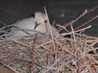
Mourning dove on nest in Tucson
(PD) Photo: John R. Brews
Mourning dove on nest in Tucson
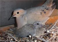
Morning dove with squab, Tucson AZ.
(PD) Photo: John R. Brews
Morning dove with squab, Tucson AZ.
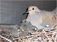
Mourning dove with squab.
(PD) Photo: John R. Brews
Mourning dove with squab.
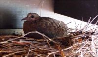
Mourning dove squab.
(PD) Photo: John R. Brews
Mourning dove squab.
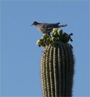
Mourning dove on saguaro cactus, Tucson AZ.
(PD) Image: John R. Brews
Mourning dove on saguaro cactus, Tucson AZ.

Magnetism

Magnetism
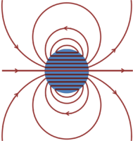
B-field lines near uniformly magnetized sphere
(CC) Image: John R. Brews
B-field lines near uniformly magnetized sphere
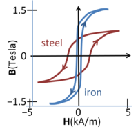
Magnetic flux density vs. magnetic field in steel and iron
(CC) Image: John R. Brews
Magnetic flux density vs. magnetic field in steel and iron
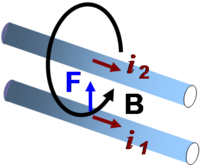
B-field from current I2 in wire 2 causes force F on wire 1.
(PD) Image: John R. Brews
B-field from current I2 in wire 2 causes force F on wire 1.

Chemistry

Chemistry
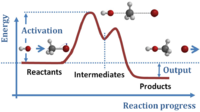
Reactants cross an energy barrier, enter an intermediate state and finally emerge in a lower energy configuration.
(PD) Image: John R. Brews
Reactants cross an energy barrier, enter an intermediate state and finally emerge in a lower energy configuration.

Circuits

Current sources
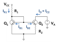
Widlar current source using bipolar transistors
(CC) Image: John R. Brews
Widlar current source using bipolar transistors
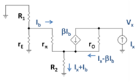
Small-signal circuit for finding output resistance of the Widlar source
(CC) Image: John R. Brews
Small-signal circuit for finding output resistance of the Widlar source
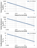
Design trade-off between output resistance and output current in Widlar source
(CC) Image: John R. Brews
Design trade-off between output resistance and output current in Widlar source
A current mirror implemented with npn bipolar transistors using a resistor to set the reference current IREF; VCC = supply voltage.
(PD) Image: John R. Brews
A current mirror implemented with npn bipolar transistors using a resistor to set the reference current IREF; VCC = supply voltage.
An n-channel MOSFET current mirror with a resistor to set the reference current
(PD) Image: John R. Brews
An n-channel MOSFET current mirror with a resistor to set the reference current
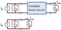
Gain-boosted current mirror with op amp feedback to increase output resistance.
(PD) Image: John R. Brews
Gain-boosted current mirror with op amp feedback to increase output resistance.
MOSFET version of wide-swing current mirror; M1 and M2 are in active mode
(PD) Image: John R. Brews
MOSFET version of wide-swing current mirror; M1 and M2 are in active mode
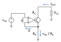
Operational-amplifier based current sink. Because the op amp is modeled as a nullor, op amp input variables are zero regardless of the values for its output variables.
(PD) Image: John R. Brews
Operational-amplifier based current sink. Because the op amp is modeled as a nullor, op amp input variables are zero regardless of the values for its output variables.
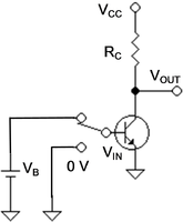
A digital inverter circuit using a bipolar transistor.
(PD) Image: John R. Brews
A digital inverter circuit using a bipolar transistor.
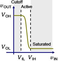
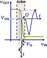
Transfer characteristic of bipolar inverter showing modes.
(PD) Image: John R. Brews
Transfer characteristic of bipolar inverter showing modes.
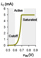
Collector current vs. input voltage for a bipolar inverter with VCC=5V and RC=1kΩ.
Input and output signals for bipolar inverter used as an amplifier.
(PD) Image: John R. Brews
Input and output signals for bipolar inverter used as an amplifier.
Two-port network with symbol definitions.
(PD) Image: John R. Brews
Two-port network with symbol definitions.
Z-equivalent two port showing independent variables I1 and I2.
(PD) Image: John R. Brews
Z-equivalent two port showing independent variables I1 and I2.
Y-equivalent two port showing independent variables
(PD) Image: John R. Brews
Y-equivalent two port showing independent variables
H-equivalent two-port showing independent variables
(PD) Image: John R. Brews
H-equivalent two-port showing independent variables
G-equivalent two-port showing independent variables
(PD) Image: John R. Brews
G-equivalent two-port showing independent variables
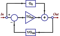
Block diagram for asymptotic gain model
(PD) Image: John R. Brews
Block diagram for asymptotic gain model
Possible signal-flow graph for the asymptotic gain model
(PD) Image: John R. Brews
Possible signal-flow graph for the asymptotic gain model
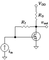
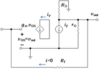
MOSFET transresistance feedback amplifier.
(PD) Image: John R. Brews
MOSFET transresistance feedback amplifier.
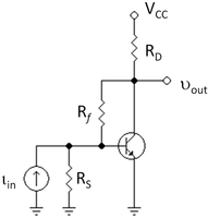
Collector-to-base biased bipolar amplifier.
(PD) Image: John R. Brews
Collector-to-base biased bipolar amplifier.
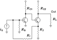
Two-transistor feedback amplifier; any source impedance RS is lumped in with the base resistor RB.
(PD) Image: John R. Brews
Two-transistor feedback amplifier; any source impedance RS is lumped in with the base resistor RB.
Small-signal circuits
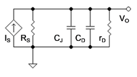
Small-signal circuit for pn-diode driven by a current signal represented as a Norton source.
(PD) Image: John R. Brews
Small-signal circuit for pn-diode driven by a current signal represented as a Norton source.
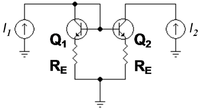
Bipolar current mirror with emitter resistors
(PD) Image: John R. Brews
Bipolar current mirror with emitter resistors
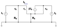
Small-signal circuit for bipolar current mirror
(PD) Image: John R. Brews
Small-signal circuit for bipolar current mirror
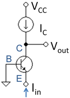
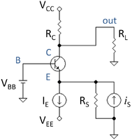
Common base circuit with active load and current drive.
(PD) Image: John R. Brews
Common base circuit with active load and current drive.
Common-base amplifier with AC current source I1 as signal input
(PD) Image: John R. Brews
Common-base amplifier with AC current source I1 as signal input
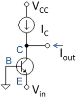
Bipolar transistor with base grounded and signal applied to emitter.
(PD) Image: John R. Brews
Bipolar transistor with base grounded and signal applied to emitter.
Common-base amplifier with AC voltage source V1 as signal input
(PD) Image: John R. Brews
Common-base amplifier with AC voltage source V1 as signal input
The result of applying Norton's theorem.
(PD) Image: John R. Brews
The result of applying Norton's theorem.
Bipolar current buffer.
(PD) Image: John R. Brews
Bipolar current buffer.
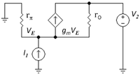
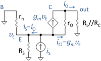
Small-signal circuit to find output current.
(PD) Image: John R. Brews
Small-signal circuit to find output current.
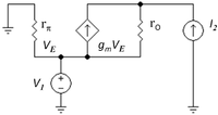
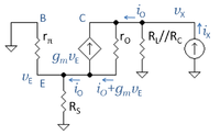
Small-signal circuit with test current iX to find Norton resistance.
(PD) Image: John R. Brews
Small-signal circuit with test current iX to find Norton resistance.
The result of applying Thévenin's theorem.
(PD) Image: John R. Brews
The result of applying Thévenin's theorem.
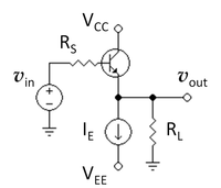
Bipolar buffer.
(PD) Image: John R. Brews
Bipolar buffer.
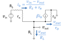
Small-signal circuit for voltage follower.
(PD) Image: John R, Brews
Small-signal circuit for voltage follower.
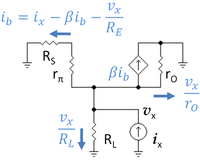
Determination of the small-signal output resistance.
(PD) Image: John R. Brews
Determination of the small-signal output resistance.
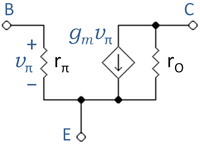
Simplified, low-frequency hybrid-pi BJT model.
(PD) Image: John R. Brews
Simplified, low-frequency hybrid-pi BJT model.
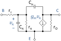
Bipolar hybrid-pi model with parasitic capacitances.
(PD) Image: John R. Brews
Bipolar hybrid-pi model with parasitic capacitances.
Simplified, low-frequency hybrid-pi BJT model.
(PD) Image: John R. Brews
Simplified, low-frequency hybrid-pi BJT model.
Bipolar hybrid-pi model with parasitic capacitances.
(PD) Image: John R. Brews
Bipolar hybrid-pi model with parasitic capacitances.
Simplified, three-terminal MOSFET hybrid-pi model.
(PD) Image: John R. Brews
Simplified, three-terminal MOSFET hybrid-pi model.
Four-terminal small-signal MOSFET circuit.
(PD) Image: John R. Brews
Four-terminal small-signal MOSFET circuit.
Miller effect: These two circuits are equivalent.
(PD) Image: John R. Brews
Miller effect: These two circuits are equivalent.
Small-signal circuit for transresistance amplifier
(PD) Image: John R. Brews
Small-signal circuit for transresistance amplifier
Small-signal circuit with return path broken and test current it driving amplifier at the break.
(PD) Image: John R. Brews
Small-signal circuit with return path broken and test current it driving amplifier at the break.
Three small-signal schematics used to discuss the asymptotic gain model
(PD) Image: John R. Brews
Three small-signal schematics used to discuss the asymptotic gain model
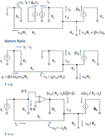
Return ratio
Left - small-signal circuit corresponding to bipolar amplifier; Center - inserting independent source and marking leads to be cut; Right - cutting the dependent source free and short-circuiting broken leads.
(PD) Image: John R. Brews
Left - small-signal circuit corresponding to bipolar amplifier; Center - inserting independent source and marking leads to be cut; Right - cutting the dependent source free and short-circuiting broken leads.
Amplifiers
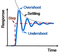
Some terms used to describe step response in time domain.
(PD) Image: John R. Brews
Some terms used to describe step response in time domain.
Ideal negative feedback model; open loop gain is AOL and feedback factor is β.
(PD) Image: John R. Brews
Ideal negative feedback model; open loop gain is AOL and feedback factor is β.
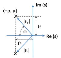
Conjugate pole locations for step response of two-pole feedback amplifier.
(PD) Image: John R. Brews
Conjugate pole locations for step response of two-pole feedback amplifier.
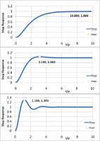
Step-response of a linear two-pole feedback amplifier.
(PD) Image: John R. Brews
Step-response of a linear two-pole feedback amplifier.
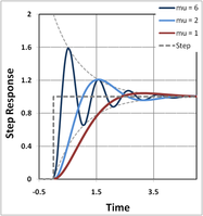
Step response for three values of time constant ratio.
(PD) Image: John R. Brews
Step response for three values of time constant ratio.
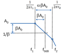
Bode gain plot to find phase margin of two-pole amplifier.
(PD) Image: John R. Brews
Bode gain plot to find phase margin of two-pole amplifier.
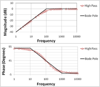
The Bode plot for a first-order (one-pole) highpass filter
(PD) Image: John R. Brews
The Bode plot for a first-order (one-pole) highpass filter
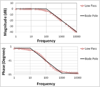
The Bode plot for a first-order (one-pole) lowpass filter
(PD) Image: John R. Brews
The Bode plot for a first-order (one-pole) lowpass filter
Bode magnitude plot for zero and for low-pass pole
(PD) Image: John R. Brews
Bode magnitude plot for zero and for low-pass pole
Bode phase plot for zero and for low-pass pole
(PD) Image: John R. Brews
Bode phase plot for zero and for low-pass pole
Bode magnitude plot for pole-zero combination; the location of the zero is ten times higher than in above figures
(PD) Image: John R. Brews
Bode magnitude plot for pole-zero combination; the location of the zero is ten times higher than in above figures
Bode phase plot for pole-zero combination; the location of the zero is ten times higher than in above figures
(PD) Image: John R. Brews
Bode phase plot for pole-zero combination; the location of the zero is ten times higher than in above figures
Gain of feedback amplifier AFB in dB and corresponding open-loop amplifier AOL.
(PD) Image: John R. Brews
Gain of feedback amplifier AFB in dB and corresponding open-loop amplifier AOL.
Phase of feedback amplifier °AFB in degrees and corresponding open-loop amplifier °AOL.
(PD) Image: John R. Brews
Phase of feedback amplifier °AFB in degrees and corresponding open-loop amplifier °AOL.
Gain of feedback amplifier AFB in dB and corresponding open-loop amplifier AOL.
(PD) Image: John R. Brews
Gain of feedback amplifier AFB in dB and corresponding open-loop amplifier AOL.
Phase of feedback amplifier AFB in degrees and corresponding open-loop amplifier AOL.
(PD) Image: John R. Brews
Phase of feedback amplifier AFB in degrees and corresponding open-loop amplifier AOL.
Operational amplifier with compensation capacitor CC between input and output to cause pole splitting.
(PD) Image: John R. Brews
Operational amplifier with compensation capacitor CC between input and output to cause pole splitting.
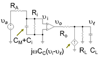
Operational amplifier with compensation capacitor transformed using Miller's theorem to replace the compensation capacitor with a Miller capacitor at the input and a frequency-dependent current source at the output.
(PD) Image: John R. Brews
Operational amplifier with compensation capacitor transformed using Miller's theorem to replace the compensation capacitor with a Miller capacitor at the input and a frequency-dependent current source at the output.
Idealized Bode plot for a two pole amplifier design.
(PD) Image: John R. Brews
Idealized Bode plot for a two pole amplifier design.
Miller capacitance at low frequencies CM (top) and compensation capacitor CC (bottom) as a function of gain
(PD) Image: John R. Brews
Miller capacitance at low frequencies CM (top) and compensation capacitor CC (bottom) as a function of gain

Logic

Logic and Venn diagrams
Venn diagrams; set A is the interior of the blue circle (left), set B is the interior of the red circle (right).
(PD) Image: John R. Brews
Venn diagrams; set A is the interior of the blue circle (left), set B is the interior of the red circle (right).
Venn diagrams; set X is the interior of the blue circle (left), set Y is the interior of the red circle (right).
(PD) Image: John R. Brews
Venn diagrams; set X is the interior of the blue circle (left), set Y is the interior of the red circle (right).
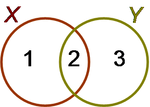
Venn diagram showing subsets of two sets X and Y.
(PD) Image: John R. Brews
Venn diagram showing subsets of two sets X and Y.
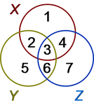
Venn diagram for three sets X, Y, and Z.
(PD) Image: John R. Brews
Venn diagram for three sets X, Y, and Z.
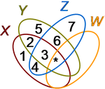
Venn diagram for four sets X, Y, Z, and W.
(PD) Image: John R. Brews
Venn diagram for four sets X, Y, Z, and W.
Venn diagram for five sets X, Y, Z, V and W.
(PD) Image: John R. Brews
Venn diagram for five sets X, Y, Z, V and W.
A three-input logic gate (center) with its Venn diagram (top) and truth table (bottom).
(PD) Image: John R. Brews
A three-input logic gate (center) with its Venn diagram (top) and truth table (bottom).
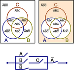
Five-switch network with Venn diagrams for branches
(PD) Image: John R. Brews
Five-switch network with Venn diagrams for branches
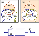
Equivalent three-switch network with Venn diagrams for branches
(PD) Image: John R. Brews
Equivalent three-switch network with Venn diagrams for branches


Forces

Forces
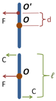
Force and its equivalent force and couple
(CC) Image: John R. Brews
Force and its equivalent force and couple
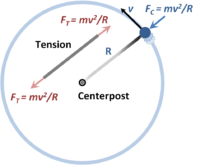
Centripetal force FC upon an object held in circular motion by a string of length R. The string is under tension FT, as shown separately to the left.
(PD) Image: John R. Brews
Centripetal force FC upon an object held in circular motion by a string of length R. The string is under tension FT, as shown separately to the left.
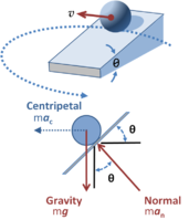
Upper panel: Ball on a banked circular track moving with constant speed v; Lower panel: Forces on the ball.
(PD) Image: John R. Brews
Upper panel: Ball on a banked circular track moving with constant speed v; Lower panel: Forces on the ball.
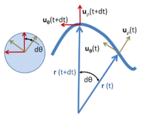
Polar unit vectors at two times t and t + dt for a particle with trajectory r ( t ); on the left the unit vectors uρ and uθ at the two times are moved so their tails all meet, and are shown to trace an arc of a unit radius circle.
(PD) Image: John R. Brews
Polar unit vectors at two times t and t + dt for a particle with trajectory r ( t ); on the left the unit vectors uρ and uθ at the two times are moved so their tails all meet, and are shown to trace an arc of a unit radius circle.
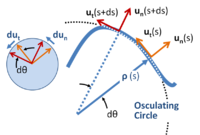
Local coordinate system for planar motion on a curve.
(PD) Image: John R. Brews
Local coordinate system for planar motion on a curve.
Exploded view of rotating spheres in an inertial frame of reference showing the centripetal forces on the spheres provided by the tension in a rope tying them together.
(PD) Image: John R. Brews
Exploded view of rotating spheres in an inertial frame of reference showing the centripetal forces on the spheres provided by the tension in a rope tying them together.
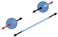
Rotating spheres subject to centrifugal (outward) force in a co-rotating frame in addition to the (inward) tension from the rope.
(PD) Image: John R. Brews
Rotating spheres subject to centrifugal (outward) force in a co-rotating frame in addition to the (inward) tension from the rope.
The "whirling table". The rod is made to rotate about the axis and (from the bead's viewpoint) the centrifugal force acting on the sliding bead is balanced by the weight attached by a cord over two pulleys.
(PD) Image: John R. Brews
The "whirling table". The rod is made to rotate about the axis and (from the bead's viewpoint) the centrifugal force acting on the sliding bead is balanced by the weight attached by a cord over two pulleys.
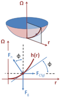
Force diagram for an element of water surface in co-rotating frame.
(PD) Image: John R. Brews
Force diagram for an element of water surface in co-rotating frame.
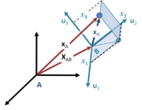
An object located at xA in inertial frame A is located at location xB in accelerating frame B.
(PD) Image: John R. Brews
An object located at xA in inertial frame A is located at location xB in accelerating frame B.
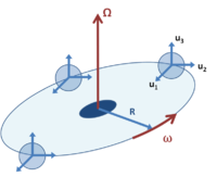
An orbiting but fixed orientation coordinate system B, shown at three different times.
(PD) Image: John R. Brews
An orbiting but fixed orientation coordinate system B, shown at three different times.
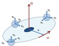
An orbiting coordinate system B in which unit vectors uj, j = 1, 2, 3 rotate to face the rotational axis.
(PD) Image: John R. Brews
An orbiting coordinate system B in which unit vectors uj, j = 1, 2, 3 rotate to face the rotational axis.
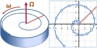
Crossing a rotating carousel walking at constant speed, a spiral is traced out in the inertial frame, while a simple straight radial path is seen in the frame of the carousel.
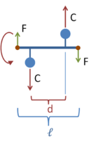
Rotating shaft unbalanced by two identical attached weights. Image
(PD) Image: John R. Brews
Rotating shaft unbalanced by two identical attached weights. Image
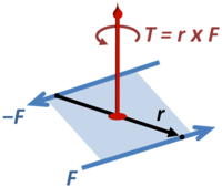
Torque vector T representing a force couple.
(PD) Image: John R. Brews
Torque vector T representing a force couple.
An ellipsoid showing its axes
(PD) Image: John R. Brews
An ellipsoid showing its axes
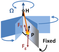
While the pendulum P swings in a fixed plane about its hanger at H, the planes of the Earth observer rotate.
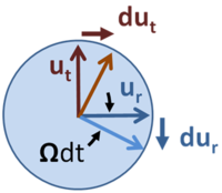
As time progresses each unit vector's change is orthogonal to it.
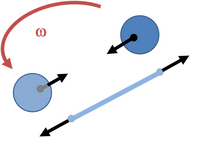
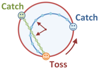
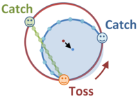
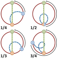
Tossed ball on carousel. At the center of the carousel, the path is a straight line for a stationary observer, and is an arc for a rotating observer.
From the center of curvature of the path, the ball executes approximate circular motion.
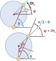
Some useful notation for the ball toss on a carousel.
The ball follows a nearly circular path about the center of curvature.
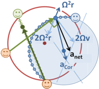
The inertial forces on the ball combine to provide the resultant centripetal force required by Newton's laws for circular motion.
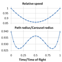
Stats for a particular path of ball toss.
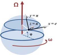
Tangent-plane coordinate system on rotating Earth at latitude φ.
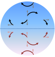
Wind motion in direction of pressure gradient is deflected by the Coriolis force.
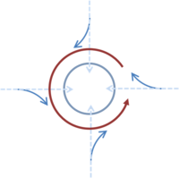
In the northern hemisphere, Coriolis force forms a counterclockwise flow.
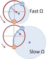
Path of ball for four rates of rotation. Catcher positioned so the catch is made at 12 o'clock in all cases.
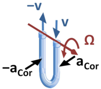
A fluid forced through a rocking tube experiences a Coriolis acceleration.

Electromagnetism

Electromagnetism
Electric motor using a current loop in a magnetic flux density, labeled B
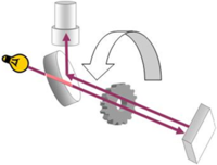
The Fizeau apparatus for measuring the speed of light by passing it between the cogs of a rotating gear and reflecting it back through adjacent cogs.
Measuring a length using interference fringes.
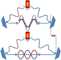
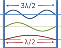
The wavelengths of standing waves in a box that have zero amplitude (nodes) at the walls.
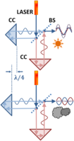
Measuring a length in wavelengths of light using a Michelson interferometer.
Boat opposing incoming waves experiences the Doppler effect
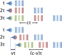
Doppler shift with moving source
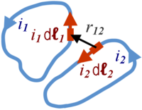
Infinitesimal current elements in two closed current-carrying loops
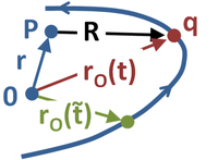
Origin at 0, observation point at P, and present position of charge q distant by R from observation point P.

Devices

Devices
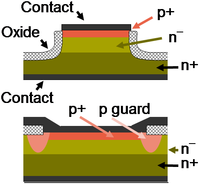
Mesa diode structure (top) and planar diode structure with guard-ring (bottom).
A planar bipolar junction transistor as might be constructed in a integrated circuit.
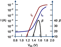
Gummel plot and current gain for a GaAs/AlGaAs heterostructure bipolar transistor.
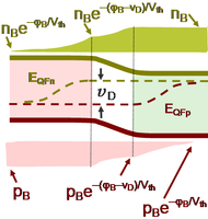
Quasi-Fermi levels and carrier densities in forward biased pn-diode.
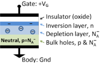
Cross section of MOS capacitor showing charge layers
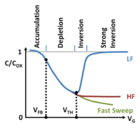
Three types of MOS capacitance vs. voltage curves. VTH = threshold, VFB = flatbands 
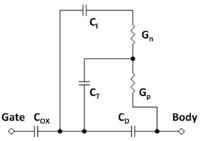
Small-signal equivalent circuit of the MOS capacitor in inversion with a single trap level
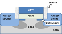
A modern MOSFET
A modern MOSFET
A power MOSFET; source and body share a contact.
Two bipolar transistor modes, showing extrapolation of asymptotes to the Early voltage.
Channel length modulation in 3/4μm technology.
Early voltage for MOSFETs from a 0.18μm process as a function of channel strength.
Calculated density of states for crystalline silicon.
Field effect: At a gate voltage above threshold a surface inversion layer of electrons forms at a semiconductor surface.
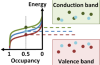
Occupancy comparison between n-type, intrinsic and p-type semiconductors.
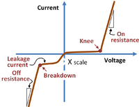
Nonideal pn-diode current-voltage characteristics
Band-bending diagram for pn-junction diode at zero applied voltage
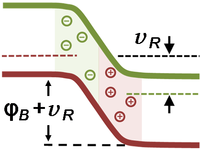
Band-bending for pn-diode in reverse bias
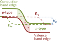
Quasi-Fermi levels in reverse-biased pn-junction diode
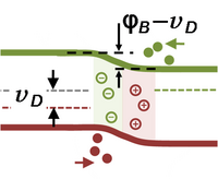
Band-bending diagram for pn-diode in forward bias
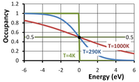
Fermi occupancy function vs. energy departure from Fermi level in volts for three temperatures
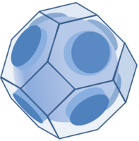
Fermi surface in k-space for a nearly filled band in the face-centered cubic lattice

More Devices

Devices
A constant energy surface in the silicon conduction band consists of six ellipsoids.
Planar Schottky diode with n+-guard rings and tapered oxide.
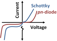
Comparison of Schottky and pn-diode current voltage curves.
Schottky barrier formation on p-type semiconductor. Energies are in eV.
Schottky diode under forward bias VF.
Schottky diode under reverse bias VR.
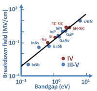
Critical electric field for breakdown versus bandgap energy in several materials.
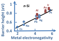
Schottky barrier height vs. metal electronegativity for some selected metals on n-type silicon.
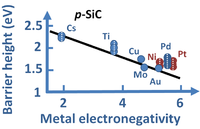
Theoretical dependence of Schottky barrier heights for diodes using p-SiC vs. electronegativity of the metal according to Mönch

Vestibular system

Vestibular system
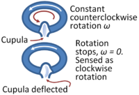
When the semicircular canal stops rotating, inertia causes the cupula to register a false rotation in the opposite sense.
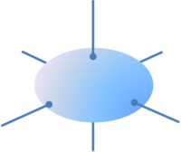
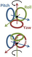
Top: The semicircular canals with head erect. Bottom: the canals with head tipped forward.